1418CG 데이터 시트보기 (PDF) - Linear Technology
부품명
상세내역
제조사
1418CG Datasheet PDF : 30 Pages
| |||
LTC1418
APPLICATIONS INFORMATION
DATA
IN
14
CLOCK
INPUT
SHIFT
REGISTER
DATA
OUT
THREE
STATE
BUFFER
SAR
16 CONVERSION CLOCK CYCLES
THREE
STATE
BUFFER
• • • 17 SCLK*
23 RD
25 CS
19 DOUT*
18 CLKOUT*
EOC
•••
16 EXTCLKIN*
20 EXT/INT*
INTERNAL
CLOCK
*PINS 16 TO 20 ARE LABELED WITH THEIR SERIAL FUNCTIONS
26 BUSY
1418 F20
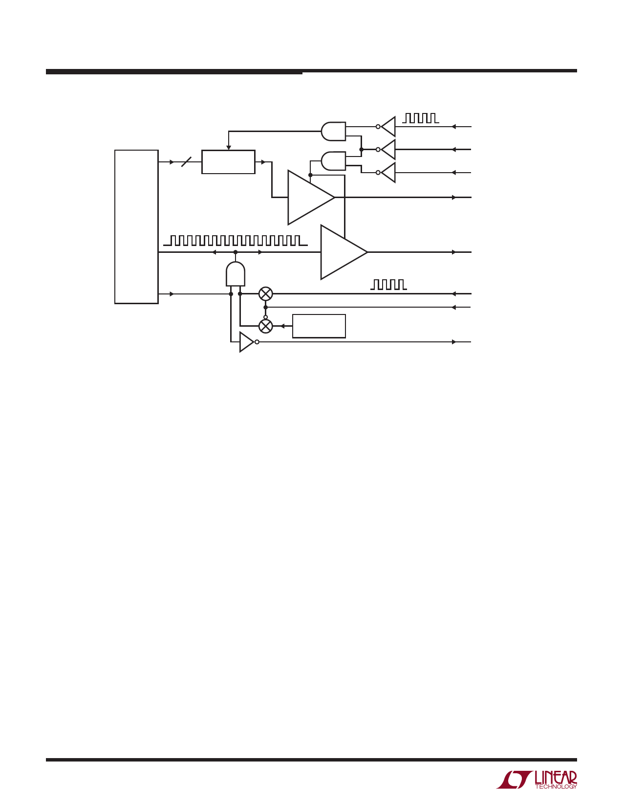
Figure 20. Functional Block Diagram for Serial Mode (SER/PAR = High)
The SCLK is used to clock the shift register. Data may be
clocked out with the internal conversion clock operating as
a master by connecting CLKOUT (Pin 18) to SCLK (Pin 17)
or with an external data clock applied to D3 (SCLK). The
minimum number of SCLK cycles required to transfer a
data word is 14. Normally, SCLK contains 16 clock cycles
for a word length of 16 bits; 14 bits with MSB first, fol-
lowed by two trailing zeros.
A logic high on RD disables SCLK and three-states DOUT. In
case of using a continuous SCLK, RD can be controlled to
limit the number of shift clocks to the desired number (i.e.,
16 cycles) and to three-state DOUT after the data transfer.
A logic high on CS three-states the DOUT output buffer.
It also inhibits conversion when it is tied high. In power
shutdown mode (SHDN = low), a high CS selects sleep
mode while a low CS selects nap mode. For normal serial
port operation, CS can be grounded.
DOUT outputs the serial data; 14 bits, MSB first, on the
falling edge of each SCLK (see Figures 21 and 22). If
16 SCLKs are provided, the 14 data bits will be followed
by two zeros. The MSB (D13) will be valid on the first
rising and the first falling edge of the SCLK. D12 will be
valid on the second rising and the second falling edge as
will all the remaining bits. The data may be captured on
either edge. The largest hold time margin is achieved if
data is captured on the rising edge of SCLK.
BUSY gives the end of conversion indication. When the
LTC1418 is configured as a master serial device, BUSY
can be used as a framing pulse and to three-state the se-
rial port after transferring the serial output data by tying
it to the RD pin.
Figures 22 to 25 show several serial modes of operation,
demonstrating the flexibility of the LTC1418 serial port.
SERIAL DATA OUTPUT DURING A CONVERSION
Using Internal Conversion Clock for Conversion and
Data Transfer
Figure 22 shows data from the previous conversion be-
ing clocked out during the conversion with the LTC1418
internal clock providing both the conversion clock and the
SCLK. The internal clock has been optimized for the fast-
est conversion time, consequently this mode can provide
the best overall speed performance. To select an internal
conversion clock, tie EXT/INT (Pin 20) low. The internal
1418fa
22
For more information www.linear.com/LTC1418
Share Link: 