LT1468(RevA) 데이터 시트보기 (PDF) - Linear Technology
부품명
상세내역
제조사
LT1468 Datasheet PDF : 16 Pages
| |||
LT1468
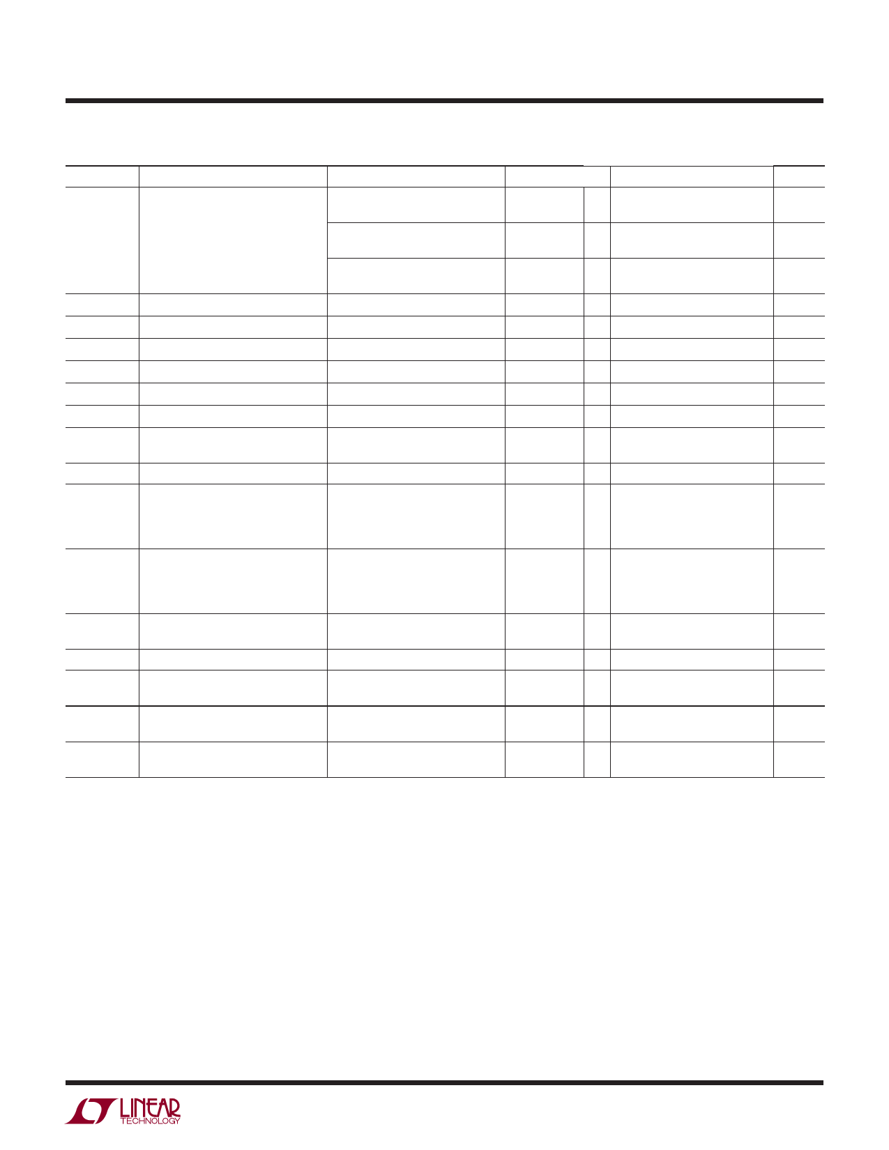
ELECTRICAL CHARACTERISTICS The l denotes the specifications which apply over the full operating
temperature range, otherwise specifications are at TA = 25°C. –40°C ≤ TA ≤ 85°C, VCM = 0V unless otherwise noted.
SYMBOL
VOS
PARAMETER
Input Offset Voltage
CONDITIONS
N8, S8
VSUPPLY
MIN
TYP
MAX
±15V
●
230
± 5V
●
330
LT1468A, DD Package
±15V
●
230
± 5V
●
330
LT1468, DD Package
±15V
●
400
± 5V
●
500
Input VOS Drift
(Note 7)
±5V to ±15V ●
0.7
2.5
IOS
Input Offset Current
±5V to ±15V ●
80
Input Offset Current Drift
IB–
Inverting Input Bias Current
±5V to ±15V
±5V to ±15V ●
120
±30
Negative Input Current Drift
IB+
Noninverting Input Bias Current
±5V to ±15V
±5V to ±15V ●
80
±60
CMRR
PSRR
AVOL
VOUT
IOUT
ISC
SR
Common Mode Rejection Ratio
Power Supply Rejection Ratio
Large-Signal Voltage Gain
Output Swing
Output Current
Short-Circuit Current
Slew Rate
VCM = ±12.5V
VCM = ±2.5V
VS = ±4.5V to ±15V
VOUT = ±12V, RL = 10k
VOUT = ±10V, RL = 2k
VOUT = ±2.5V, RL = 10k
VOUT = ±2.5V, RL = 2k
RL = 10k
RL = 2k
RL = 10k
RL = 2k
VOUT = ±12.5V
VOUT = ±2.5V
VOUT = 0V, VIN = ±0.2V
AV = –1, RL = 2k (Note 5)
±15V
±5V
±15V
±15V
±5V
±5V
±15V
±15V
±5V
±5V
±15V
±5V
±15V
±15V
±5V
● 92
● 92
● 96
● 300
● 150
● 300
● 150
● ±12.8
● ±12.6
● ±2.8
● ±2.6
● ±7
● ±7
● ±12
●
9
●
6
GBW
Gain Bandwidth
f = 100kHz, RL = 2k
±15V
±5V
● 45
● 40
IS
Supply Current
±15V
●
7.0
±5V
●
6.8
UNITS
μV
μV
μV
μV
μV
μV
μV/°C
nA
pA/°C
nA
pA/°C
nA
dB
dB
dB
V/mV
V/mV
V/mV
V/mV
V
V
V
V
mA
mA
mA
V/μs
V/μs
MHz
MHz
mA
mA
Note 1: Stresses beyond those listed under Absolute Maximum Ratings
may cause permanent damage to the device. Exposure to any Absolute
Maximum Rating condition for extended periods may affect device
reliability and lifetime.
Note 2: The inputs are protected by back-to-back diodes and two 100Ω
series resistors. If the differential input voltage exceeds 0.7V, the input
current should be limited to 10mA. Input voltages outside the supplies will
be clamped by ESD protection devices and input currents should also be
limited to 10mA.
Note 3: A heat sink may be required to keep the junction temperature
below absolute maximum when the output is shorted indefinitely.
Note 4: The LT1468C is guaranteed to meet specified performance from
0°C to 70°C and is designed, characterized and expected to meet these
extended temperature limits, but is not tested at – 40°C and at 85°C. The
LT1468I is guaranteed to meet the extended temperature limits.
Note 5: Slew rate is measured between ±8V on the output with ±12V input
for ±15V supplies and ±2V on the output with ±3V input for ±5V supplies.
Note 6: Full power bandwidth is calculated from the slew rate
measurement: FPBW = SR/2πVP
Note 7: This parameter is not 100% tested.
1468fa
5
Share Link: 