ISL6526CRZ-T 데이터 시트보기 (PDF) - Intersil
부품명
상세내역
제조사
ISL6526CRZ-T Datasheet PDF : 15 Pages
| |||
ISL6526, ISL6526A
The maximum RMS current required by the regulator may be
closely approximated through the following equation:
IRMSMAX =
V-----O----U---T-
VIN
×
⎛
⎝
IO
UTM
A
2
X
+
--1----
12
×
⎛
⎝
-V----I-N-----–-----V----O----U---T-
L × fs
×
V---V--O--I--UN---T-⎠⎞
2⎞
⎠
(EQ. 8)
For a through hole design, several electrolytic capacitors may
be needed. For surface mount designs, solid tantalum
capacitors can be used, but caution must be exercised with
regard to the capacitor surge current rating. These capacitors
must be capable of handling the surge-current at power-up.
Some capacitor series available from reputable manufacturers
are surge current tested.
MOSFET Selection/Considerations
The ISL6526, ISL6526A require two N-Channel power
MOSFETs. These should be selected based upon rDS(ON),
gate supply requirements, and thermal management
requirements.
In high-current applications, the MOSFET power dissipation,
package selection and heatsink are the dominant design
factors. The power dissipation includes two loss components;
conduction loss and switching loss. The conduction losses are
the largest component of power dissipation for both the upper
and the lower MOSFETs. These losses are distributed between
the two MOSFETs according to duty factor. The switching
losses seen when sourcing current will be different from the
switching losses seen when sinking current. When sourcing
current, the upper MOSFET realizes most of the switching
losses. The lower switch realizes most of the switching losses
when the converter is sinking current (see equations on next
page). These equations assume linear voltage-current
transitions and do not adequately model power loss due the
reverse-recovery of the upper and lower MOSFET’s body
diode. The gate-charge losses are dissipated by the ISL6526,
ISL6526A and don't heat the MOSFETs. However, large gate-
charge increases the switching interval, tSW which increases
the MOSFET switching losses. Ensure that both MOSFETs are
within their maximum junction temperature at high ambient
temperature by calculating the temperature rise according to
package thermal-resistance specifications. A separate heatsink
may be necessary depending upon MOSFET power, package
type, ambient temperature and air flow.
Losses while Sourcing current
PUPPER
=
I
o2
×
rDS(O
N)
×
D
+
1--
2
⋅
I
o
×
VI
N
×
tS
W
×
fs
PLOWER = Io2 x rDS(ON) x (1 - D)
Losses while Sinking current
PUPPER = Io2 x rDS(ON) x D
PLOWER
=
I
o2
×
rD
S
(
O
N
)
×
(
1
–
D
)
+
1--
2
⋅
I
o
×
VIN
×
tS
W
×
fs
Where: D is the duty cycle = VOUT / VIN,
tSW is the combined switch ON and OFF time, and
fs is the switching frequency.
(EQ. 9)
Given the reduced available gate bias voltage (5V), logic-
level or sub-logic-level transistors should be used for both
N-MOSFETs. Caution should be exercised with devices
exhibiting very low VGS(ON) characteristics. The shoot-
through protection present aboard the ISL6526, ISL6526A
may be circumvented by these MOSFETs if they have large
parasitic impedances and/or capacitances that would inhibit
the gate of the MOSFET from being discharged below its
threshold level before the complementary MOSFET is turned
on.
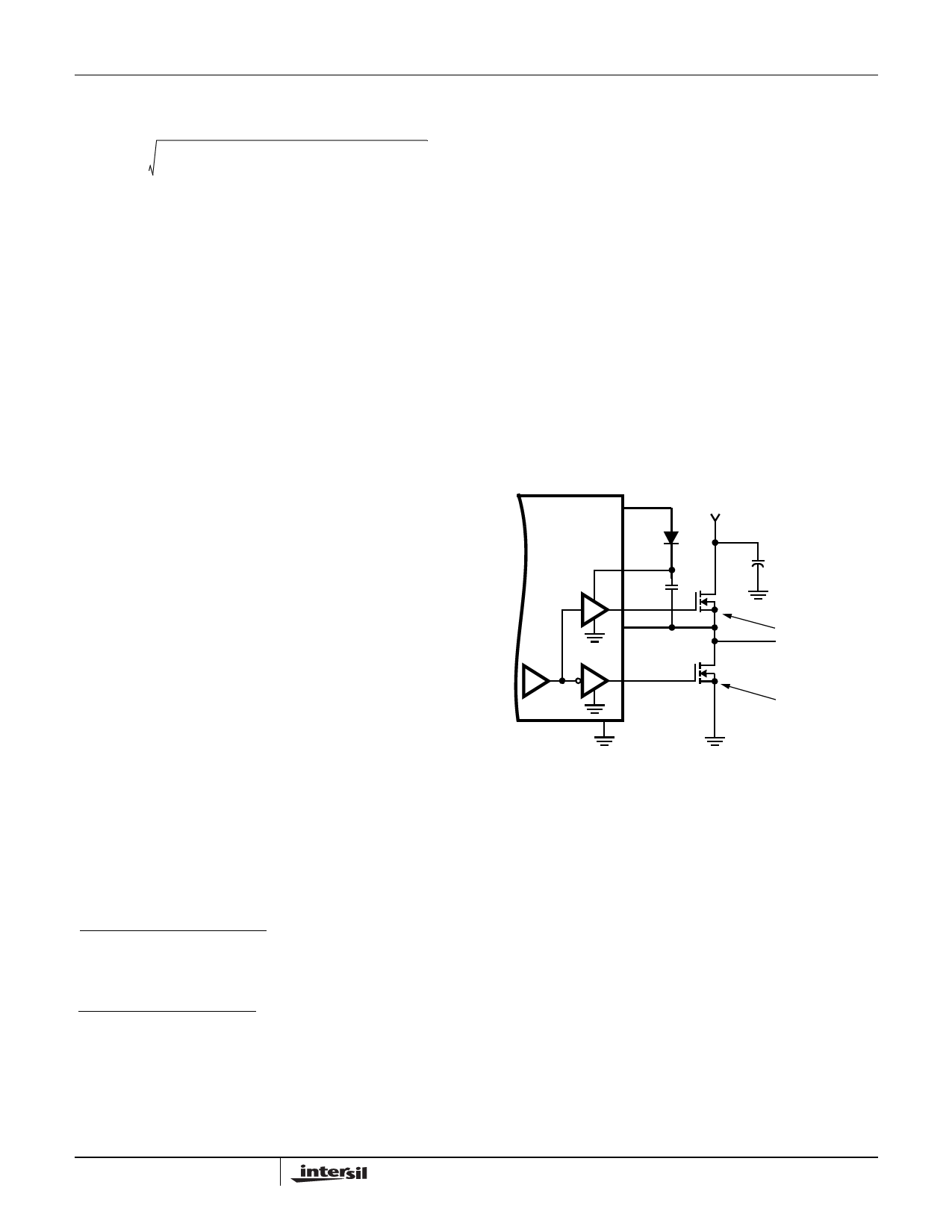
Bootstrap Component Selection
External bootstrap components, a diode and capacitor, are
required to provide sufficient gate enhancement to the upper
MOSFET. The internal MOSFET gate driver is supplied by
the external bootstrap circuitry as shown in Figure 7. The
boot capacitor, CBOOT, develops a floating supply voltage
referenced to the PHASE pin. This supply is refreshed each
cycle, when DBOOT conducts, to a voltage of CPVOUT less
the boot diode drop, VD, plus the voltage rise across
QLOWER.
ISL6526,
ISL6526A
CPVOUT
DBOOT +
VD
VIN
-
BOOT
CBOOT
UGATE
PHASE
QUPPER
NOTE:
VG-S = VCC -VD
-
LGATE
QLOWER
+
GND
NOTE:
VG-S = VCC
FIGURE 7. UPPER GATE DRIVE BOOTSTRAP
Just after the PWM switching cycle begins and the charge
transfer from the bootstrap capacitor to the gate capacitance
is complete, the voltage on the bootstrap capacitor is at its
lowest point during the switching cycle. The charge lost on
the bootstrap capacitor will be equal to the charge
transferred to the equivalent gate-source capacitance of the
upper MOSFET as shown:
QGATE = CBOOT × (VBOOT1 – VBOOT2)
(EQ. 10)
where QGATE is the maximum total gate charge of the upper
MOSFET, CBOOT is the bootstrap capacitance, VBOOT1 is
the bootstrap voltage immediately before turn-on, and
VBOOT2 is the bootstrap voltage immediately after turn-on.
The bootstrap capacitor begins its refresh cycle when the gate
drive begins to turn-off the upper MOSFET. A refresh cycle
12
FN9055.8
March 20, 2007
Share Link: 