IDT70V16S 데이터 시트보기 (PDF) - Integrated Device Technology
부품명
상세내역
제조사
IDT70V16S Datasheet PDF : 18 Pages
| |||
PRELIMINARYPRE
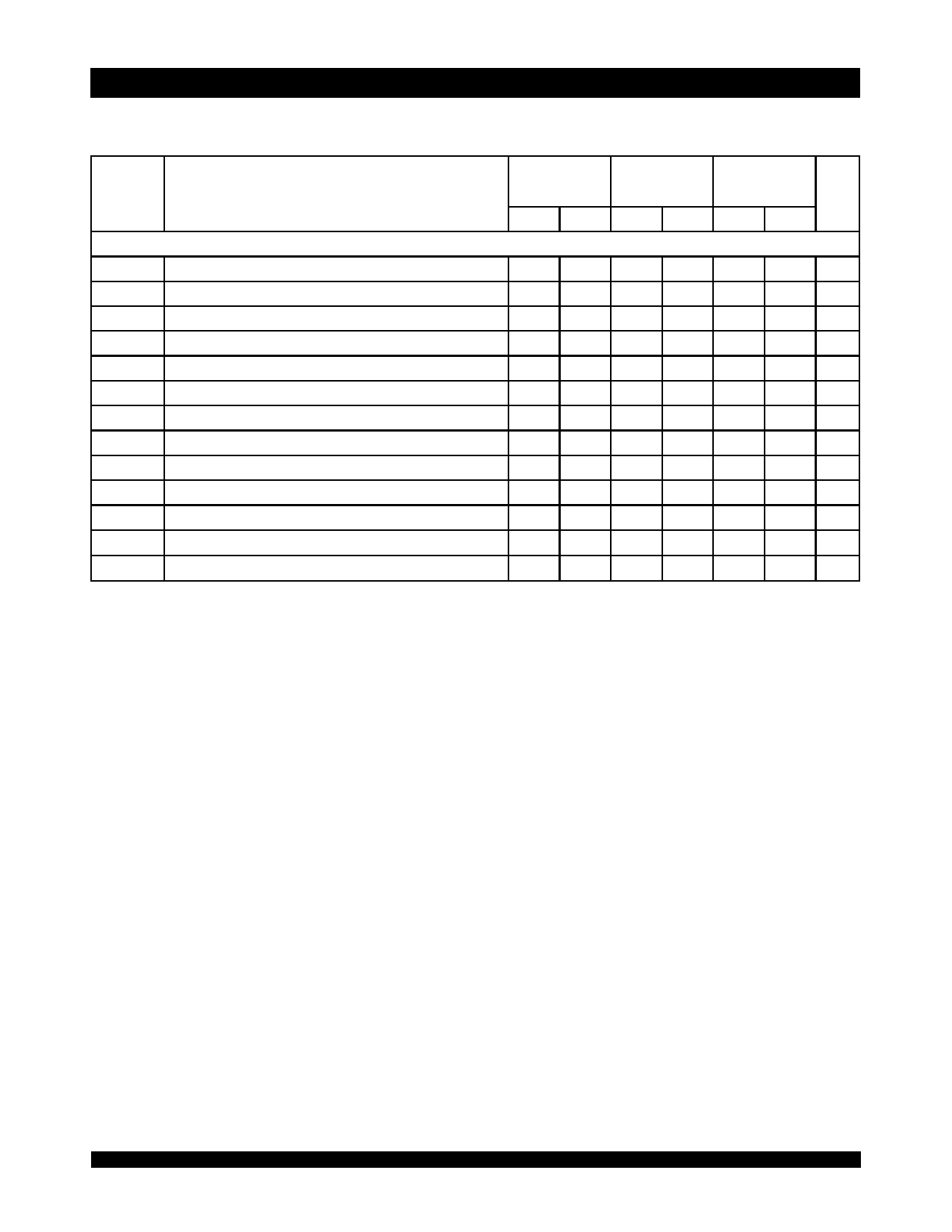
IDT70V16/5S/L
High-Speed 3.3V 16/8K x 9 Dual-Port Static RAM
PRELIMINARY
Industrial and Commercial Temperature Ranges
AC Electrical Characteristics Over the
Operating Temperature and Supply Voltage(5)
70V16/5X15
Com'l Only
70V16/5X20
Com'l
& Ind
70V16/5X25
Com'l Only
Symbol
Parameter
Min. Max. Min. Max. Min. Max. Unit
WRITE CYCLE
tWC
Write Cycle Time
15
____
20
____
25
____
ns
tEW
Chip Enable to End-of-Write(3)
12
____
15
____
20
____
ns
tAW
Address Valid to End-of-Write
12
____
15
____
20
____
ns
tAS
Address Set-up Time(3)
0
____
0
____
0
____
ns
tWP
Write Pulse Width
12
____
15
____
20
____
ns
tWR
Write Recovery Time
0
____
0
____
0
____
ns
tDW
Data Valid to End-of-Write
tHZ
Output High-Z Time(1,2)
tDH
Data Hold Time(4)
10
____
15
____
15
____
ns
____
10
____
12
____
15
ns
0
____
0
____
0
____
ns
tWZ
Write Enable to Output in High-Z(1,2)
tOW
Output Active from End-of-Write(1,2,4)
____
10
____
12
____
15
ns
0
____
0
____
0
____
ns
tSWRD
SEM Flag Write to Read Time
5
____
5
____
5
____
ns
tSPS
SEM Flag Contention Window
5
____
5
____
5
____
ns
NOTES:
5669 tbl 12
1. Transition is measured 0mV from Low or High-impedance voltage with the Output Test Load (Figure 2).
2. This parameter is guaranteed by device characterization but not production tested.
3. To access SRAM, CE = VIL and SEM = VIH. To access semaphore, CE = VIH and SEM = VIL. Either condition must be valid for the entire tEW time.
4. The specification for tDH must be met by the device supplying write data to the SRAM under all operating conditions. Although tDH and tOW values will vary over
voltageand temperature, the actual tDH will always be smaller than the actual tOW.
5. 'X' in part numbers indicates power rating (S or L).
6.482
Share Link: 