ICS8308I 데이터 시트보기 (PDF) - Integrated Circuit Systems
부품명
상세내역
제조사
ICS8308I Datasheet PDF : 15 Pages
| |||
Integrated
Circuit
Systems, Inc.
ICS8308I
LOW SKEW, 1-TO-8
DIFFERENTIAL/LVCMOS-TO-LVCMOS FANOUT BUFFER
GENERAL DESCRIPTION
The ICS8308I is a low-skew, 1-to-8 Fanout Buffer
and a member of the HiPerClockS™ family of
High Performance Clock Solutions from ICS. The
ICS8308I has two selectable clock inputs. The
CLK, nCLK pair can accept most differential input
levels. The LVCMOS_CLK can accept LVCMOS or LVTTL
input levels. The low impedance LVCMOS/LVTTL outputs
are designed to drive 50Ω series or parallel terminated
transmission lines. The effective fanout can be increased
from 8 to 16 by utilizing the ability of the outputs to drive two
series terminated transmission lines.
The ICS8308I is characterized for 3.3V core/3.3V output,
3.3V core/2.5V output or 2.5V core/2.5V output operation.
Guaranteed output and part-part skew characteristics make
the 8308I ideal for those clock distribution applications requiring
well defined performance and repeatability.
FEATURES
• 8 LVCMOS/LVTTL outputs (7Ω typical output impedance)
• Selectable LVCMOS_CLK or differential CLK, nCLK
inputs
• CLK, nCLK pair can accept the following differential
input levels: LVPECL, LVDS, LVHSTL, SSTL, HCSL
• Maximum Output Frequency: 350MHz
• Output Skew: (3.3V± 5%): 100ps (maximum)
• Part to Part Skew: (3.3V± 5%): 1ns (maximum)
• Supply Voltage Modes:
(Core/Output)
3.3V/3.3V
3.3V/2.5V
2.5V/2.5V
• -40°C to 85°C ambient operating temperature
• Available in both, Standard and RoHS/Lead-Free
compliant packages
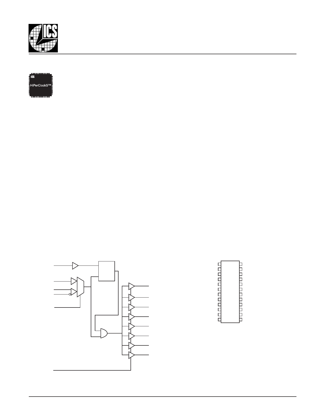
BLOCK DIAGRAM
CLK_EN Pullup
LVCMOS_CLK Pullup
1
CLK Pullup
nCLK Pulldown
0
CLK_SEL Pullup
D
Q
LE
OE Pullup
PIN ASSIGNMENT
Q0 1
24 VDDO
GND 2
23 Q2
CLK_SEL 3
22 GND
LVCMOS_CLK 4
21 Q3
Q0
CLK 5
20 VDDO
nCLK 6
19 Q4
Q1
CLK_EN 7
18 GND
OE 8
17 Q5
Q2
VDD 9
16 VDDO
GND 10 15 Q6
Q3
Q1 11 14 GND
VDDO 12 13 Q7
Q4
ICS8308I
Q5
24-Lead, 300-MIL TSSOP
Q6
4.4mm x 7.8mm x 0.92mm body package
G Package
Q7
Top View
8308AGI
www.icst.com/products/hiperclocks.html
1
REV. B JULY 25, 2005
Share Link: 