HEF4044BP 데이터 시트보기 (PDF) - NXP Semiconductors.
부품명
상세내역
제조사
HEF4044BP Datasheet PDF : 13 Pages
| |||
NXP Semiconductors
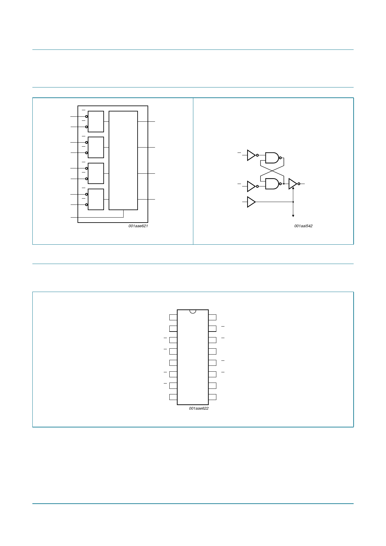
5. Functional diagram
HEF4044B
Quad R/S latch with 3-state outputs
3 1S
4 1R
1Q 13
7 2S
6 2R
11 3S
12 3R
2Q 9
3-STATE
OUTPUTS
3Q 10
15 4S
14 4R
5 OE
Fig 1. Functional diagram
4Q 1
001aae621
6. Pinning information
6.1 Pinning
nS
nR
nQ
OE
to other latches
001aai542
Fig 2. Logic diagram for one latch
Fig 3. Pin configuration
HEF4044B
4Q 1
n.c. 2
1S 3
1R 4
OE 5
2R 6
2S 7
VSS 8
16 VDD
15 4S
14 4R
13 1Q
12 3R
11 3S
10 3Q
9 2Q
001aae622
HEF4044B_6
Product data sheet
Rev. 06 — 11 November 2008
© NXP B.V. 2008. All rights reserved.
2 of 13
Share Link: 