CAT5261YI-00-T2(2009) 데이터 시트보기 (PDF) - ON Semiconductor
부품명
상세내역
제조사
CAT5261YI-00-T2
(Rev.:2009)
(Rev.:2009)
ON Semiconductor
CAT5261YI-00-T2 Datasheet PDF : 15 Pages
| |||
CAT5261
Dual Digitally Programmable Potentiometers
(DPP™) with 256 Taps and SPI Interface
FEATURES
Two linear-taper digitally programmable
potentiometers
256 resistor taps per potentiometer
End to end resistance 50 kΩ or 100 kΩ
Potentiometer control and memory access via
SPI interface
Low wiper resistance, typically 100
Nonvolatile memory storage for up to four
wiper settings for each potentiometer
Automatic recall of saved wiper settings at
power up
2.5 to 6.0 volt operation
Standby current less than 1µA
1,000,000 nonvolatile WRITE cycles
100 year nonvolatile memory data retention
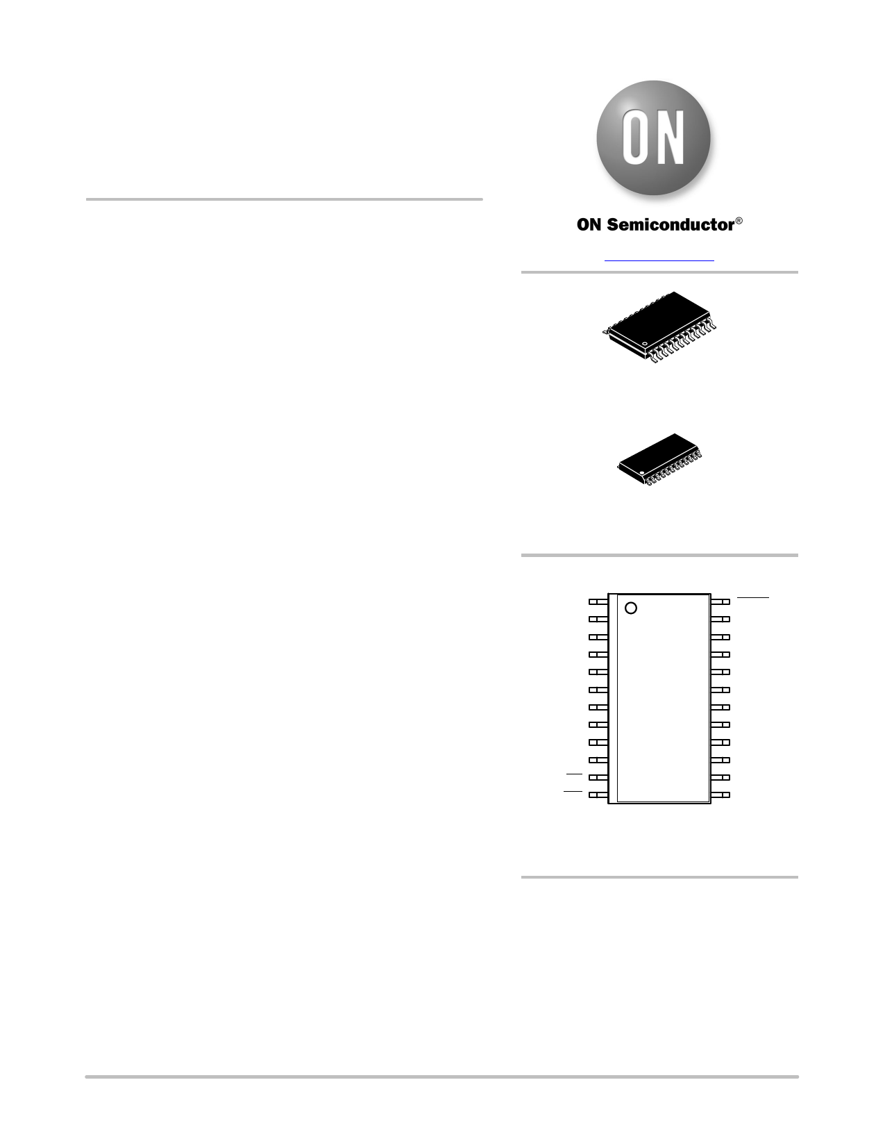
24-lead SOIC and 24-lead TSSOP
Industrial temperature range
Industrial temperature range
For Ordering Information details, see page 14.
DESCRIPTION
The CAT5261 is two Digitally Programmable
Potentiometers (DPPs™) integrated with control logic
and 8 bytes of NVRAM memory. Each DPP consists of
a series of resistive elements connected between two
externally accessible end points. The tap points
between each resistive element are connected to the
wiper outputs with CMOS switches. A separate 8-bit
control register (WCR) independently controls the wiper
tap switches for each DPP. Associated with each wiper
control register are four 8-bit non-volatile memory data
registers (DR) used for storing up to four wiper settings.
Writing to the wiper control register or any of the non-
volatile data registers is via a SPI serial bus. On power-
up, the contents of the first data register (DR0) for each
of the potentiometers is automatically loaded into its
respective wiper control register.
The CAT5261 can be used as a potentiometer or as a
two terminal, variable resistor. It is intended for circuit
level or system level adjustments in a wide variety of
applications. It is available in the -40°C to 85°C
industrial operating temperature range and offered in
a 24-lead SOIC and TSSOP package.
PIN CONFIGURATION
SOIC/TSSOP (W, Y)
SO 1
24 H¯¯O¯L¯D¯
A0 2
23 SCK
NC 3
22 NC
NC 4
21 NC
NC 5
20 NC
NC
6
CAT
5261
19
NC
VCC 7
18 GND
RL0 8
17 RW1
RH0 9
16 RH1
RW0 10
¯C¯S¯ 11
15 RL1
14 A1
¯W¯P¯ 12
13 SI
FUNCTIONAL DIAGRAM
RH0 RH1
CS
SCK
SI
SO
SPI BUS
INTERFACE
WIPER
CONTROL
REGISTERS
RW0
WP
A0
A1
HOLD
CONTROL
LOGIC
NONVOLATILE
DATA
REGISTERS
RL0 RL1
RW1
© 2009 SCILLC. All rights reserved.
1
Characteristics subject to change without notice
Doc. No. MD-2122 Rev. G
Share Link: 