C8051F006 데이터 시트보기 (PDF) - Unspecified
부품명
상세내역
제조사
C8051F006 Datasheet PDF : 170 Pages
| |||
PRELIMINARY
C8051F000/1/2/5/6/7
C8051F010/1/2/5/6/7
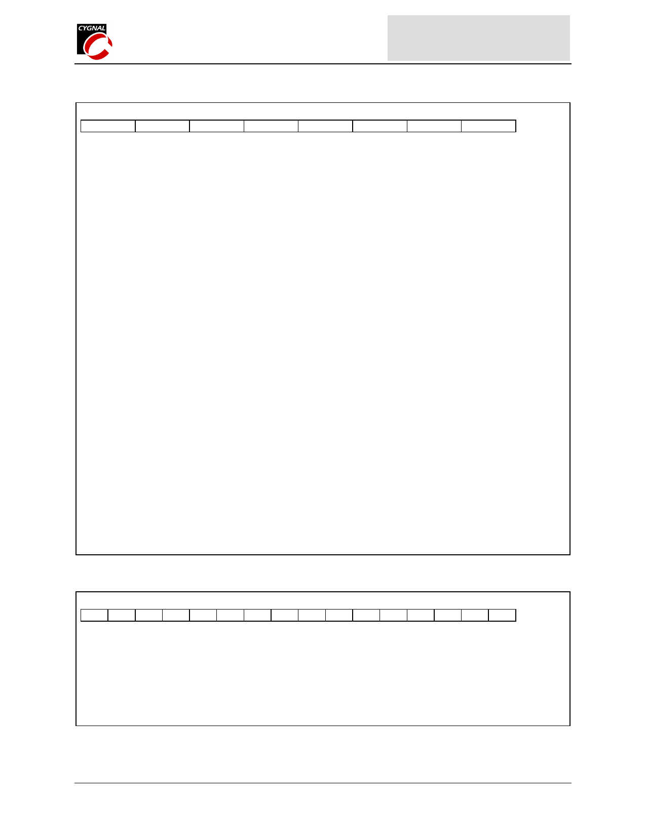
Figure 21.3. FLASHCON: JTAG Flash Control Register
WRMD3
Bit7
WRMD2
Bit6
WRMD1
Bit5
WRMD0
Bit4
RDMD3
Bit3
RDMD2
Bit2
RDMD1
Bit1
RDMD0
Bit0
Reset Value
00000000
This register determines how the Flash interface logic will respond to reads and writes to the
FLASHDAT Register.
Bits7-4: WRMD3-0: Write Mode Select Bits.
The Write Mode Select Bits control how the interface logic responds to writes to the
FLASHDAT Register per the following values:
0000: A FLASHDAT write replaces the data in the FLASHDAT register, but is otherwise
ignored.
0001: A FLASHDAT write initiates a write of FLASHDAT into the memory location
addressed by the FLASHADR register. FLASHADR is incremented by one when
complete.
0010: A FLASHDAT write initiates an erasure (sets all bytes to 0xFF) of the Flash page
containing the address in FLASHADR. FLASHDAT must be 0xA5 for the erase to
occur. FLASHADR is not affected. If FLASHADR = 0x7DFE – 0x7DFF, the entire
user space will be erased (i.e. entire Flash memory except for Reserved area 0x7E00 –
0x7FFF).
(All other values for WRMD3-0 are reserved.)
Bits3-0: RDMD3-0: Read Mode Select Bits.
The Read Mode Select Bits control how the interface logic responds to reads to the
FLASHDAT Register per the following values:
0000: A FLASHDAT read provides the data in the FASHDAT register, but is otherwise
ignored.
0001: A FLASHDAT read initiates a read of the byte addressed by the FLASHADR register
if no operation is currently active. This mode is used for block reads.
0010: A FLASHDAT read initiates a read of the byte addressed by FLASHADR only if no
operation is active and any data from a previous read has already been read from
FLASHDAT. This mode allows single bytes to be read (or the last byte of a block)
without initiating an extra read.
(All other values for RDMD3-0 are reserved.)
Figure 21.4. FLASHADR: JTAG Flash Address Register
Reset Value
0x0000
Bit15
Bit0
This register holds the address for all JTAG Flash read, write, and erase operations. This register
autoincrements after each read or write, regardless of whether the operation succeeded or failed.
Bits15-0: Flash Operation 16-bit Address.
Page 166
CYGNAL Integrated Products, Inc. 2001
4.2001; Rev. 1.3
Share Link: 