AON2408 데이터 시트보기 (PDF) - Unspecified
부품명
상세내역
제조사
AON2408 Datasheet PDF : 5 Pages
| |||
AON2408
20V N-Channel MOSFET
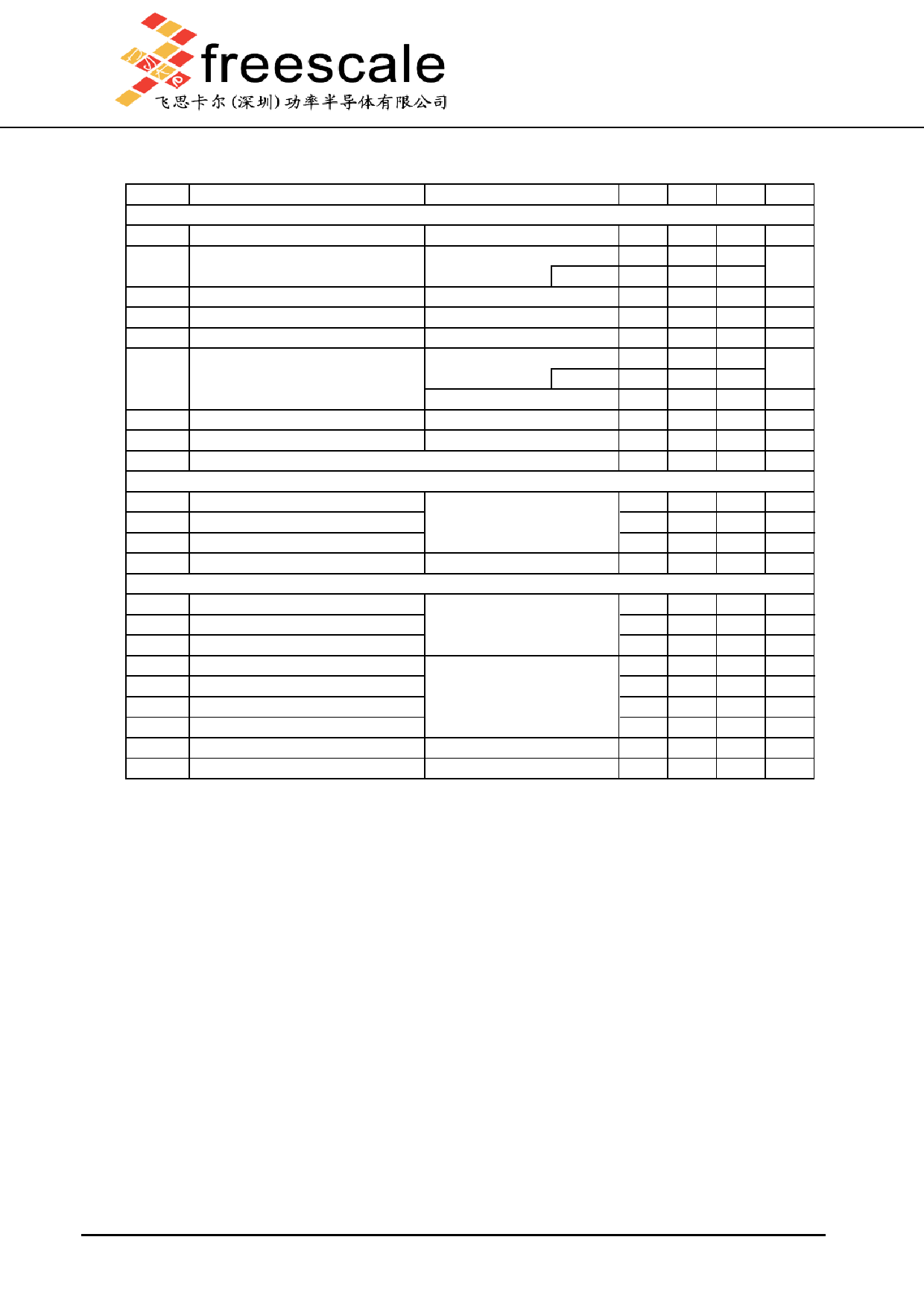
Electrical Characteristics (TJ=25°C unless otherwise noted)
Symbol
Parameter
Conditions
Min Typ Max Units
STATIC PARAMETERS
BVDSS Drain-Source Breakdown Voltage
ID=250µA, VGS=0V
20
V
IDSS
Zero Gate Voltage Drain Current
VDS=20V, VGS=0V
TJ=55°C
1
µA
5
IGSS
Gate-Body leakage current
VDS=0V, VGS=±12V
±100 nA
VGS(th) Gate Threshold Voltage
VDS=VGS, ID=250µA
0.5 0.83 1.2
V
ID(ON)
On state drain current
VGS=4.5V, VDS=5V
32
A
RDS(ON) Static Drain-Source On-Resistance
VGS=4.5V, ID=8A
TJ=125°C
11.6 14.5
mΩ
16.3 20.5
VGS=2.5V, ID=4A
15
19 mΩ
gFS
Forward Transconductance
VDS=5V, ID=8A
50
S
VSD
Diode Forward Voltage
IS=1A,VGS=0V
0.65 1
V
IS
Maximum Body-Diode Continuous Current
3.5
A
DYNAMIC PARAMETERS
Ciss
Input Capacitance
Coss
Output Capacitance
Crss
Reverse Transfer Capacitance
Rg
Gate resistance
VGS=0V, VDS=10V, f=1MHz
VGS=0V, VDS=0V, f=1MHz
782
pF
158
pF
98
pF
2.4
Ω
SWITCHING PARAMETERS
Qg
Total Gate Charge
7
nC
Qgs
Gate Source Charge
VGS=4.5V, VDS=10V, ID=8A
1
nC
Qgd
Gate Drain Charge
2.4
nC
tD(on)
Turn-On DelayTime
3
ns
tr
Turn-On Rise Time
VGS=4.5V, VDS=10V, RL=1.25Ω,
4.5
ns
tD(off)
Turn-Off DelayTime
RGEN=3Ω
28
ns
tf
Turn-Off Fall Time
6
ns
trr
Body Diode Reverse Recovery Time IF=8A, dI/dt=100A/µs
11
ns
Qrr
Body Diode Reverse Recovery Charge IF=8A, dI/dt=100A/µs
2.7
nC
A. The value of RθJA is measured with the device mounted on 1in2 FR-4 board with 2oz. Copper, in a still air environment with TA =25°C.
The Power dissipation PDSM is based on R θJA t ≤ 10s value and the maximum allowed junction temperature of 150°C. The value in any
given application depends on the user's specific board design.
B. The power dissipation PD is based on TJ(MAX)=150°C, using junction-to-case thermal resistance, and is more useful in setting the upper
dissipation limit for cases where additional heatsinking is used.
C. Repetitive rating, pulse width limited by junction temperature TJ(MAX)=150°C. Ratings are based on low frequency and duty cycles to keep
initial TJ =25°C.
D. The RθJA is the sum of the thermal impedance from junction to case RθJC and case to ambient.
E. The static characteristics in Figures 1 to 6 are obtained using <300µs pulses, duty cycle 0.5% max.
F. These curves are based on the junction-to-case thermal impedance which is measured with the device mounted to a large heatsink,
assuming a maximum junction temperature of TJ(MAX)=150°C. The SOA curve provides a single pulse rating.
G. The maximum current rating is package limited.
H. These tests are performed with the device mounted on 1 in2 FR-4 board with 2oz. Copper, in a still air environment with TA=25°C.
2/5
www.freescale.net.cn
Share Link: 