AM79C984AKC 데이터 시트보기 (PDF) - Advanced Micro Devices
부품명
상세내역
제조사
AM79C984AKC Datasheet PDF : 44 Pages
| |||
PRELIMINARY
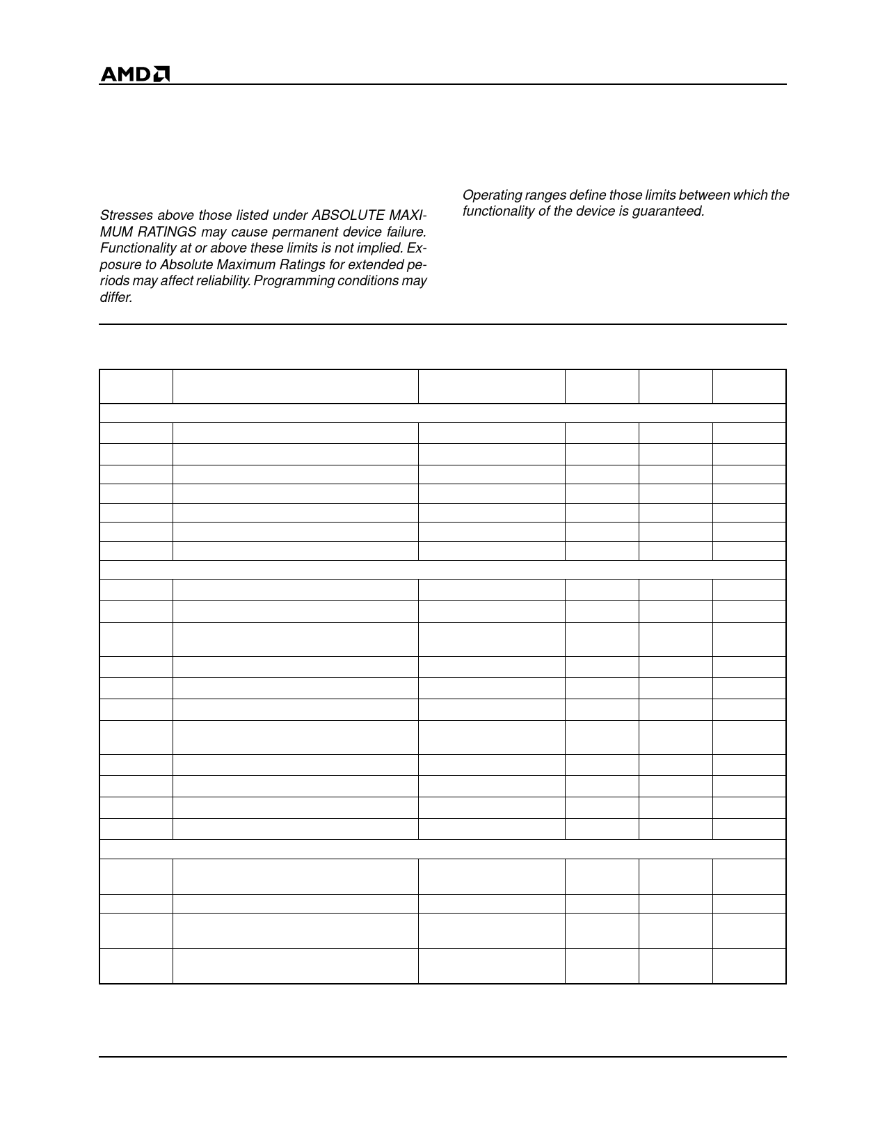
ABSOLUTE MAXIMUM RATINGS
Storage Temperature . . . . . . . . . . –65° C to +150° C
Ambient Temperature Under Bias . . . . 0° C to +70° C
Supply Voltage referenced to
AVSS or DVSS (AVDD, DVDD) . . . . . . . –0.3 V to +6.0 V
Stresses above those listed under ABSOLUTE MAXI-
MUM RATINGS may cause permanent device failure.
Functionality at or above these limits is not implied. Ex-
posure to Absolute Maximum Ratings for extended pe-
riods may affect reliability. Programming conditions may
differ.
OPERATING RANGES
Commercial (C) Devices
Temperature (TA) . . . . . . . . . . . . . . . . . 0° C to +70° C
Supply Voltages (VDD) . . . . . . . . . . . . . . . . . +5 V ±5%
Operating ranges define those limits between which the
functionality of the device is guaranteed.
DC CHARACTERISTICS over operating ranges unless otherwise specified
Parameter
Symbol
Parameter Description
Digital I/O
VIL Input LOW Voltage
VIH Input HIGH Voltage
VOL
VOH
IIL
IILSTR
VOLOD
AUI Ports
Output LOW Voltage
Output HIGH Voltage
Input Leakage Current
Input Leakage Current for STR pin
Open Drain Output LOW Voltage (LED pins)
IIAXD Input Current at DI± and CI± Pairs
VAICM DI±, CI± Open Circuit Input Voltage Range
VAIDV
Differential Mode Input Voltage Range
(DI, CI)
VASQ DI, CI Squelch Threshold
VATH DI Switching Threshold
VAOD Differential Output Voltage (DO+) – (DO)
VAOC
Differential Output Voltage (CI+) – (CI–)
(Reverse Mode)
VAODI DO Differential Output Voltage Imbalance
VAODOFF DO Differential Idle Output Voltage
IAODOFF DO Differential Idle Output Current
VAOCM DO+, DO- Common Mode Output Voltage
Twisted Pair Ports
IIRXD
Input Current at RXD±
and CI± Pairs
RRXD
VTIVB
RXD Differential Input
RXD+, RXD– Open Circuit
Input Voltage (bias)
VTID
Differential Mode Input
Range (RXD)
Test Conditions
VSS = 0.0 V
VSS = 0.0 V
IOL = 4.0 mA
IOH = –0.4 mA
VSS<VIN<VDD
VSS<VIN<VDD
IOLOD = 12 mA
VSS<VIN<VDD
IIN = 0
VDD = 5.0 V
–
(Note 1)
RL = 78 Ω
RL = 78 Ω
RL = 78 Ω
RL = 78 Ω
RL = 78 Ω (Note 1)
RL = 78 Ω
AVSS<VIN<VDD
(Note 1)
VDD = 5.0 V
Min
Max
Unit
–0.5
0.8
V
2.0
0.5 + VDD
V
–
0.4
V
2.4
–
V
–
10
µA
–
50
µA
–
0.4
V
–500
500
µA
VDD – 3.0 VDD – 1.0
V
–2.5
+2.5
V
–275
–160
mV
-35
+35
mV
620
1100
mV
620
1100
mV
–25
+25
mV
–40
+40
mV
–1.0
+1.0
mA
2.5
VDD
V
–500
500
µA
10
–
kΩ
VDD – 3.0 VDD – 1.5
V
–3.1
+3.1
V
32
Am79C984A
Share Link: 