ADT75BRMZ-REEL7(RevB) 데이터 시트보기 (PDF) - Analog Devices
부품명
상세내역
제조사
ADT75BRMZ-REEL7 Datasheet PDF : 24 Pages
| |||
ADT75
SERIAL INTERFACE
Control of the ADT75 is carried out via the SMBus/I2C-compatible
serial interface. The ADT75 is connected to this bus as a slave
and is under the control of a master device.
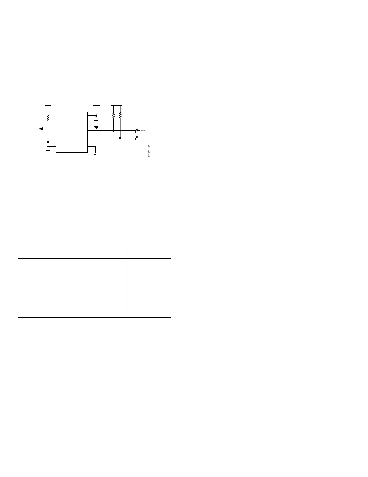
Figure 13 shows a typical SMBus/I2C interface connection.
PULL-UP
VDD
PULL-UP
VDD
VDD
10kΩ
ADT75
OS/ALERT SCL
A0
SDA
A1
A2
GND
10kΩ
0.1µF
10kΩ
SMBus/I2C ADDRESS = 1001 000
Figure 13. Typical SMBus/I2C Interface Connection
Serial Bus Address
Like all SMBus/I2C-compatible devices, the ADT75 has a 7-bit
serial address. The four MSBs of this address for the ADT75 are
set to 1001. Pin A2, Pin A1, and Pin A0 set the three LSBs. These
pins can be configured two ways, low and high, to give eight
different address options. Table 12 shows the different bus address
options available. Recommended pull-up resistor value on the
SDA and SCL lines is 10 kΩ.
Table 12. SMBus/I2C Bus Address Options
Binary
A6 A5 A4 A3 A2 A1 A0
1001000
1001001
1001010
1001011
1001100
1001101
1001110
1001111
Hex
0x48
0x49
0x4A
0x4B
0x4C
0x4D
0x4E
0x4F
The ADT75 is designed with a SMBus/I2C timeout. The
SMBus/I2C interface times out after 75 ms to 325 ms of no
activity on the SDA line. After this timeout, the ADT75 resets
the SDA line back to its idle state (SDA set to high impedance)
and wait for the next start condition.
Data Sheet
The serial bus protocol operates as follows:
1. The master initiates data transfer by establishing a start
condition, defined as a high to low transition on the serial
data line SDA, while the serial clock line SCL remains high.
This indicates that an address/data stream is going to
follow. All slave peripherals connected to the serial bus
respond to the start condition and shift in the next eight
bits, consisting of a 7-bit address (MSB first) plus a
read/write (R/W) bit. The R/W bit determines whether
data is written to, or read from, the slave device.
2. The peripheral with the address corresponding to the
transmitted address responds by pulling the data line low
during the low period before the ninth clock pulse, known
as the acknowledge bit. All other devices on the bus now
remain idle while the selected device waits for data to be
read from or written to it. If the R/W bit is a zero then the
master writes to the slave device. If the R/W bit is a one
then the master reads from the slave device.
3. Data is sent over the serial bus in sequences of nine clock
pulses, eight bits of data followed by an acknowledge bit
from the receiver of data. Transitions on the data line must
occur during the low period of the clock signal and remain
stable during the high period, as a low to high transition
when the clock is high can be interpreted as a stop signal.
4. When all data bytes have been read or written, stop
conditions are established. In write mode, the master pulls
the data line high during the 10th clock pulse to assert a
stop condition. In read mode, the master device pulls the
data line high during the low period before the ninth clock
pulse. This is known as no acknowledge. The master takes
the data line low during the low period before the 10th
clock pulse, then high during the 10th clock pulse to assert
a stop condition.
Any number of bytes of data can be transferred over the serial
bus in one operation. However, it is not possible to mix read
and write in one operation because the type of operation is
determined at the beginning and cannot subsequently be
changed without starting a new operation.
The I2C address set up by the three address pins is not latched
by the device until after this address has been sent twice. On the
eighth SCL cycle of the second valid communication, the serial
bus address is latched in. This is the SCL cycle directly after the
device has seen its own I2C serial bus address. Any subsequent
changes on this pin has no effect on the I2C serial bus address.
Rev. B | Page 16 of 24
Share Link: 