ADG701BRMZ-REEL71 데이터 시트보기 (PDF) - Analog Devices
부품명
상세내역
제조사
ADG701BRMZ-REEL71 Datasheet PDF : 12 Pages
| |||
ADG701L/ADG702L
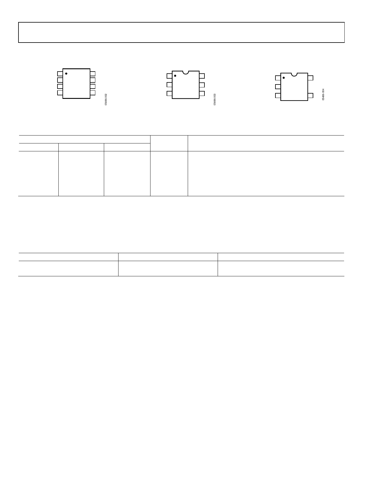
PIN CONFIGURATIONS AND FUNCTION DESCRIPTIONS
D1
8S
NC 2 ADG701L/ 7 GND
NC 3 ADG702L 6 IN
TOP VIEW
VDD 4 (Not to Scale) 5 NC
NC = NO CONNECT
Figure 3. 8-Lead MSOP Pin Configuration
D1
6 VDD
ADG701L/
S 2 ADG702L 5 NC
TOP VIEW
GND 3 (Not to Scale) 4 IN
NC = NO CONNECT
Figure 4. 6-Lead SOT-23 Pin Configuration
D1
5 VDD
ADG701L/
S 2 ADG702L
TOP VIEW
GND 3 (Not to Scale) 4 IN
Figure 5. 5-Lead SOT-23 Pin Configuration
Table 4. Pin Function Descriptions
Pin Number
8-Lead MSOP 6-lead SOT-23 5-lead SOT-23
1
1
1
2, 3, 5
5
N/A
4
6
5
6
4
4
7
3
3
8
2
2
Mnemonic
D
NC
VDD
IN
GND
S
Description
Drain Terminal. May be an input or output.
No Connect.
Most Positive Power Supply Potential.
Logic Control Input.
Ground (0 V) Reference.
Source Terminal. May be an input or output.
Table 5. Truth Table
ADG701L In
0
1
ADG702L In
1
0
Switch Condition
Off
On
Rev. 0 | Page 6 of 12
Share Link: 