AD8134ACPZ-R2(RevB) 데이터 시트보기 (PDF) - Analog Devices
부품명
상세내역
제조사
AD8134ACPZ-R2 Datasheet PDF : 20 Pages
| |||
AD8134
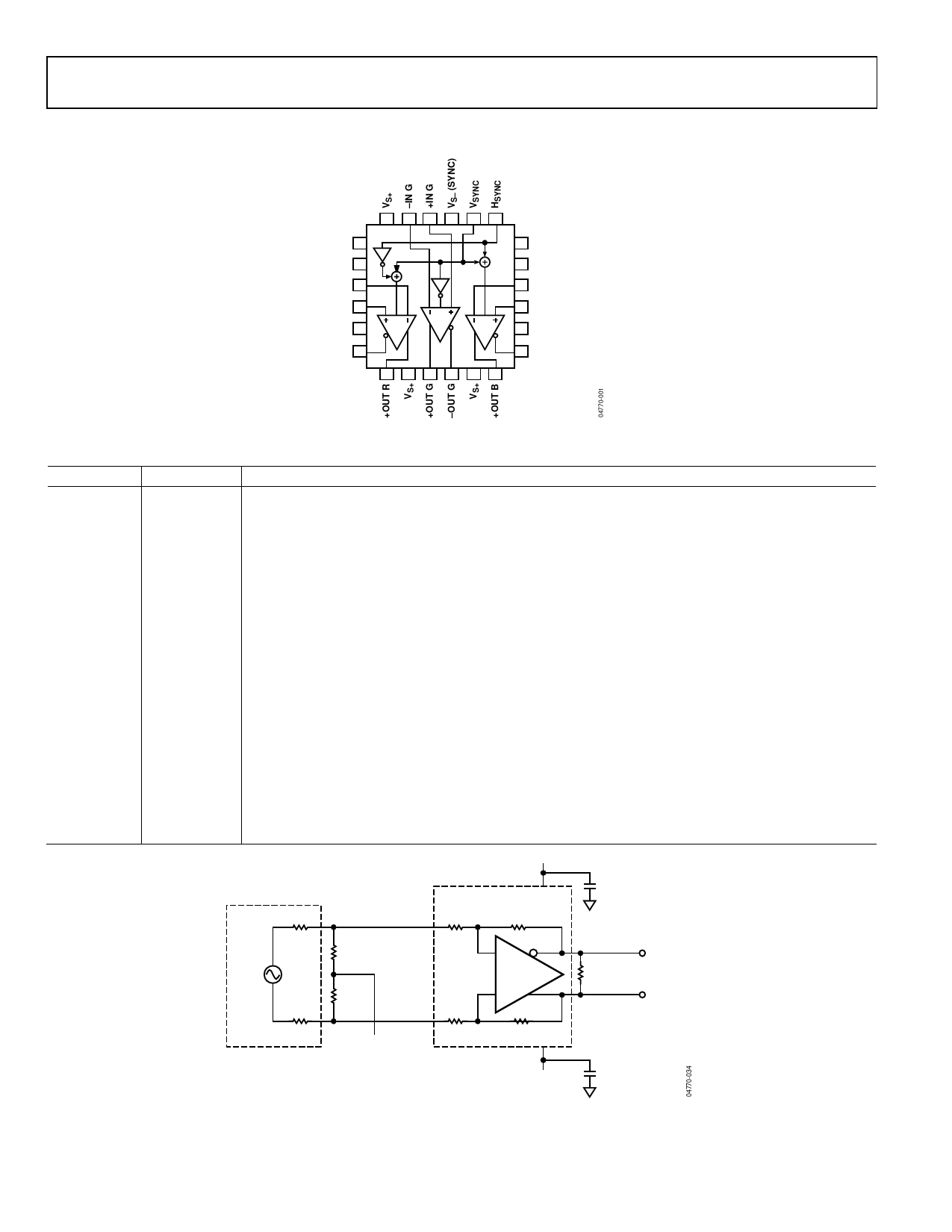
PIN CONFIGURATION AND FUNCTION DESCRIPTIONS
Data Sheet
OPD 1
VS– 2
–IN R 3
+IN R 4
VS– 5
–OUT R 6
AD8134
TOP VIEW
18 SYNC LEVEL
17 VS+ (SYNC)
16 –IN B
15 +IN B
14 VS–
13 –OUT B
NOTES
1. EXPOSED PAD. THE EXPOSED PADDLE MUST BE SOLDERED TO A PAD
ON TOP OF THE BOARD THAT IS CONNECTED TO AN INNER PLANE
WITH SEVERAL THERMAL VIAS.
Figure 4. 24-Lead LFCSP
Table 5. Pin Function Descriptions
Pin No.
Mnemonic Description
1
OPD
Output Pull Down.
2, 5, 14, 21 VS−
Negative Power Supply Voltage.
3
−IN R
Inverting Input, Red Amplifier.
4
+IN R
Noninverting Input, Red Amplifier.
6
−OUT R
Negative Output, Red Amplifier.
7
+OUT R
Positive Output, Red Amplifier.
8, 11, 17, 24 VS+
Positive Power Supply Voltage.
9
+OUT G
Positive Output, Green Amplifier.
10
−OUT G
Negative Output, Green Amplifier.
12
+OUT B
Positive Output, Blue Amplifier.
13
−OUT B
Negative Output, Blue Amplifier.
15
+IN B
Noninverting Input, Blue Amplifier.
16
−IN B
Inverting Input, Blue Amplifier.
18
SYNC LEVEL The voltage applied to this pin controls the amplitude of the sync pulses that are applied to
the common-mode voltages.
19
HSYNC
Horizontal Sync Pulse Input.
20
VSYNC
Vertical Sync Pulse Input.
22
+IN G
Noninverting Input, Green Amplifier.
23
−IN G
Inverting Input, Green Amplifier.
EPAD
Exposed Pad. The exposed paddle must be soldered to a pad on top of the board that is connected to an
inner plane with several thermal vias.
Rev. B | Page 6 of 20
Share Link: 