AD7911ARM(Rev0) 데이터 시트보기 (PDF) - Analog Devices
부품명
상세내역
제조사
AD7911ARM Datasheet PDF : 28 Pages
| |||
AD7911/AD7921
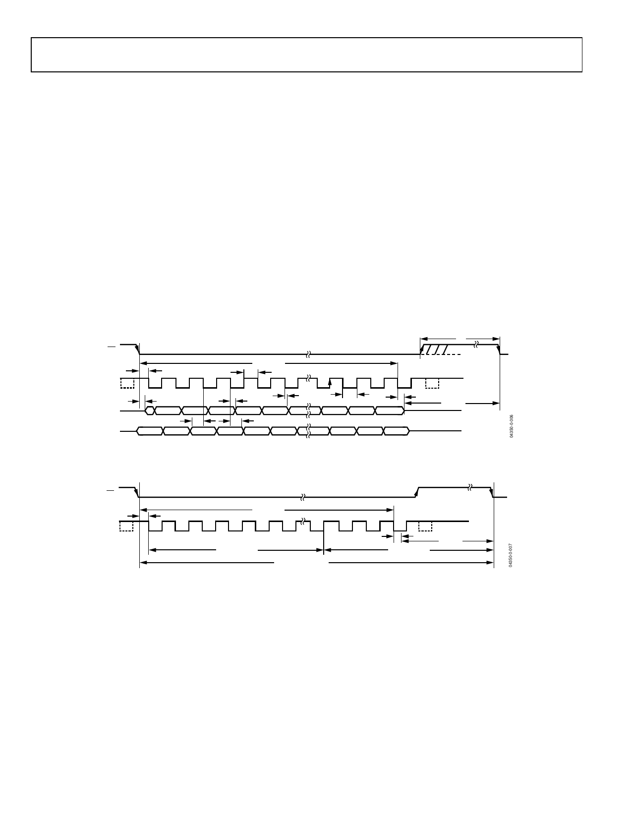
TIMING EXAMPLES
Figure 6 and Figure 7 show some of the timing parameters from
the Timing Specifications section.
Timing Example 1
As shown in Figure 7, when fSCLK = 5 MHz and the throughput is
250 kSPS, the cycle time is
t2 + 12.5(1/fSCLK) + tACQ = 4 µs
With t2 = 10 ns minimum, then tACQ is 1.49 µs, which satisfies
the requirement of 290 ns for tACQ.
In Figure 7, tACQ is comprised of 2.5(1/fSCLK) + t10 + tQUIET, where
t10 = 30 ns maximum. This allows a value of 960 ns for tQUIET,
satisfying the minimum requirement of 30 ns.
Timing Example 2
The AD7921 can also operate with slower clock frequencies. As
shown in Figure 7, when fSCLK = 2 MHz and the throughput rate
is 100 KSPS, the cycle time is
t2 + 12.5(1/fSCLK) + tACQ = 10 µs
With t2 = 10 ns minimum, then tACQ is 3.74 µs, which satisfies
the requirement of 290 ns for tACQ.
In Figure 7, tACQ is comprised of 2.5(1/fSCLK) + t10 + tQUIET, where
t10 = 30 ns maximum. This allows a value of 2.46 µs for tQUIET,
satisfying the minimum requirement of 30 ns.
In this example, as with other slower clock values, the signal
might already be acquired before the conversion is complete,
but it is still necessary to leave 30 ns minimum tQUIET between
conversions. In this example, the signal should be fully acquired
at approximately point C in Figure 7.
CS
SCLK
t2
1
2
3
t3
DOUT
Z ZERO
THREE-STATE
DIN
X
X
CHN
t8
CHN
tCONVERT
t6
4
5
t4
X
DB11
t9
X
X
t7
DB10
X
t1
B
13
14
15
16
t5
DB2 DB1
DB0
t10
tQUIET
THREE-STATE
X
X
X
Figure 6. AD7921 Serial Interface Timing Diagram
CS
SCLK
t2
tCONVERT
1
2
3
4
5
12.5(1/fSCLK)
B
13
C
14
15
16
t10
tACQUISITION
tQUIET
1/THROUGHPUT
Figure 7. Serial Interface Timing Example
Rev. 0 | Page 8 of 28
Share Link: 