AD7091 데이터 시트보기 (PDF) - Analog Devices
부품명
상세내역
제조사
AD7091 Datasheet PDF : 20 Pages
| |||
AD7091
Data Sheet
MODES OF OPERATION
The mode of operation of the AD7091 is selected by controlling
the logic level of the CONVST signal when a conversion is complete.
The two modes of operation are normal mode and power-down
mode. These modes of operation provide flexible power manage-
ment options, allowing optimization of the power dissipation to
throughput rate ratio for different application requirements.
The logic level of the CONVST pin at the end of a conversion
determines whether the AD7091 remains in normal mode or
enters power-down mode (see the Normal Mode section and the
Power-Down Mode section). Similarly, if the device is in power-
down mode, CONVST controls whether the device returns to
normal mode or remains in power-down mode.
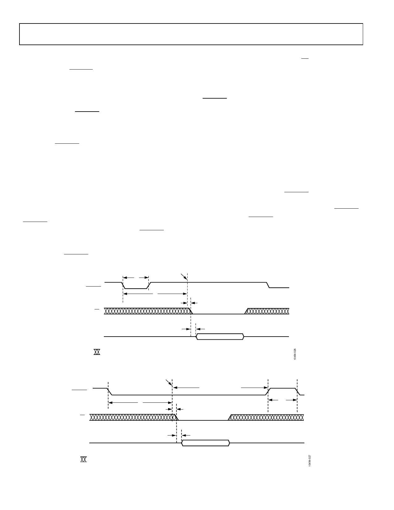
Normal Mode
The normal mode of operation is intended to achieve the fastest
throughput rate performance. In normal mode, the AD7091
remains fully powered at all times, so power-up times are not
a concern. Figure 20 shows the general timing diagram of the
AD7091 in normal mode.
In normal mode, the conversion is initiated on the falling edge of
CONVST, as described in the Serial Interface section. To ensure
that the part remains fully powered at all times, CONVST must
return high after t7 and remain high until the conversion is com-
plete. At the end of a conversion (denoted as EOC in Figure 20),
the logic level of CONVST is tested.
CONVST
EOC
t7
t8
CS
To read back data stored in the conversion result register, wait until
the conversion is complete, and then pull CS low. The conversion
data is subsequently clocked out on the SDO pin (see Figure 20).
Because the output shift register is 12 bits wide, data is shifted out
of the device as a 12-bit word under the control of the serial clock
input (SCLK). After reading back the data, the user can pull
CONVST low again to start another conversion after the tQUIET
time has elapsed.
Power-Down Mode
The power-down mode of operation is intended for use in applica-
tions where slower throughput rates and lower power consumption
are required. In this mode, the ADC can be powered down after
each conversion or after a series of conversions performed at a
high throughput rate, with the ADC powered down for relatively
long durations between these bursts of several conversions. When
the AD7091 is in power-down mode, the serial interface remains
active even though all analog circuitry is powered down.
To enter power-down mode, pull CONVST low and keep it low
prior to the end of a conversion (denoted as EOC in Figure 21).
After the conversion is complete, the logic level of the CONVST
pin is tested. If the CONVST signal is logic low, the part enters
power-down mode.
The serial interface of the AD7091 is functional in power-down
mode; therefore, users can read back the conversion result after
the part enters power-down mode.
t12
SDO
t10
CONVERSION DATA
NOTES
1. IS DON’T CARE.
2. EOC IS THE END OF A CONVERSION.
Figure 20. Normal Mode of Operation, Serial Interface Read Timing
CONVST
CS
EOC
POWER-DOWN MODE
t8
t13
t12
SDO
t10
CONVERSION DATA
NOTES
1. IS DON’T CARE.
2. EOC IS THE END OF A CONVERSION.
Figure 21. Entering and Exiting Power-Down Mode
Rev. B | Page 12 of 20
Share Link: 