AD5555CRU(Rev0) 데이터 시트보기 (PDF) - Analog Devices
부품명
상세내역
제조사
AD5555CRU Datasheet PDF : 16 Pages
| |||
AD5545/AD5555
Table 8 shows that each DAC A and DAC B can be individually
loaded with a new data value. In addition, a common new data
value can be loaded into both DACs simultaneously by setting Bit
A1 = A0 = high. This command enables the parallel combination
of both DACs, with IOUTA and IOUTB tied together, to act as one
DAC with significant improved noise performance.
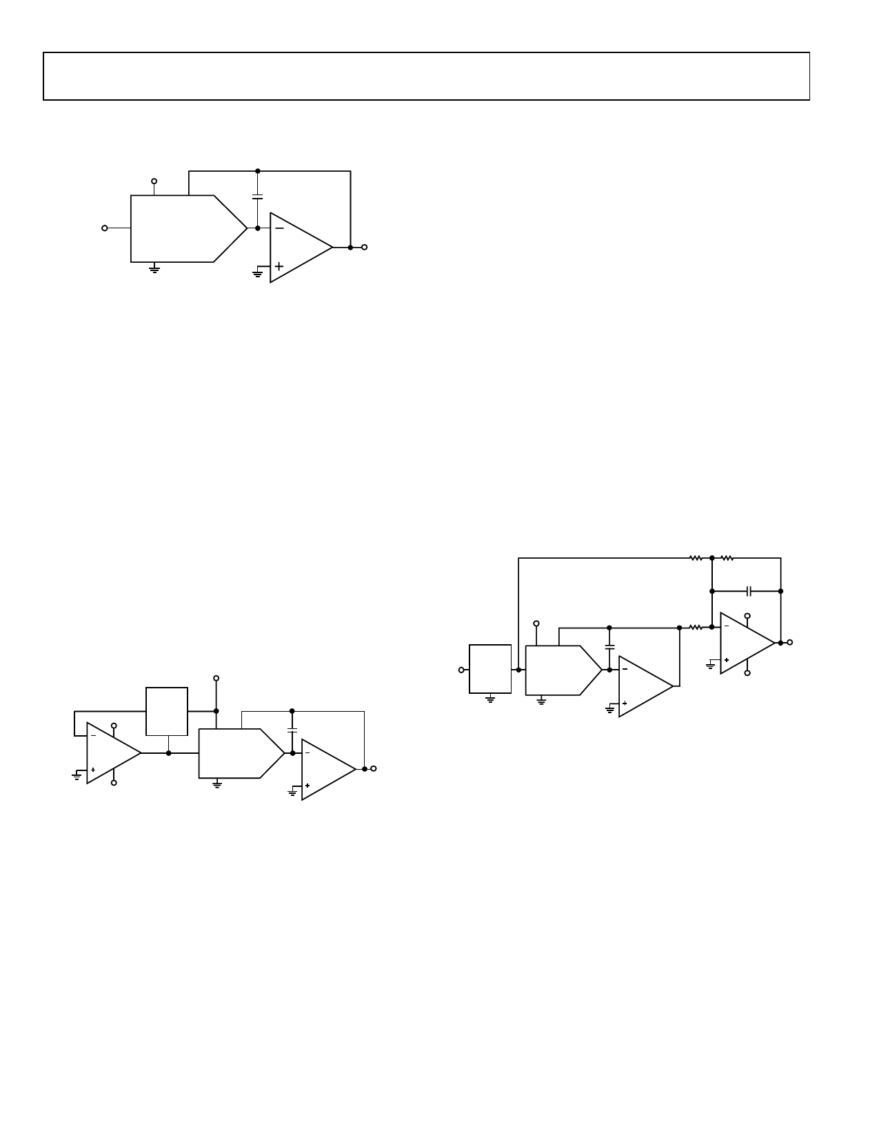
ESD Protection Circuits
All logic input pins contain back-biased ESD protection Zeners
connected to digital ground (DGND) and VDD as shown in
Figure 18.
VDD
DIGITAL
INPUTS
5kΩ
DGND
02918-0-007
Figure 18. Equivalent ESD Protection Circuits
POWER-UP SEQUENCE
It is recommended to power-up VDD and ground prior to any
reference voltages. The ideal power-up sequence is AGNDX,
DGND, VDD, VREFX, and digital inputs. A noncompliance power-
up sequence can elevate reference current, but the device will
resume normal operation once VDD is powered.
LAYOUT AND POWER SUPPLY BYPASSING
It is a good practice to employ compact, minimum lead length
layout design. The input leads should be as direct as possible
with a minimum conductor length. Ground paths should have
low resistance and low inductance.
Similarly, it is also good practice to bypass the power supplies
with quality capacitors for optimum stability. Supply leads to the
device should be bypassed with 0.01 µF to 0.1 µF disc or chip
ceramic capacitors. Low ESR 1 µF to 10 µF tantalum or electro-
lytic capacitors should also be applied at VDD to minimize any
transient disturbance and to filter any low frequency ripple
(see Figure 19). Users should not apply switching regulators for
VDD due to the power supply rejection ratio degradation over
frequency.
VDD
C2
+ C1
10µF
0.1µF
AD5545/
AD5555
VDD
AGNDX
DGND
02918-0-008
Figure 19. Power Supply Bypassing and Grounding Connection
GROUNDING
The DGND and AGNDX pins of the AD5545/AD5555 refer to the
digital and analog ground references. To minimize the digital
ground bounce, the DGND terminal should be joined remotely
at a single point to the analog ground plane (see Figure 19).
Rev. 0 | Page 12 of 16
Share Link: 