74LV163D 데이터 시트보기 (PDF) - Philips Electronics
부품명
상세내역
제조사
74LV163D Datasheet PDF : 14 Pages
| |||
Philips Semiconductors
Presettable synchronous 4-bit binary counter;
synchronous reset
Product specification
74LV163
AC WAVEFORMS
VM = 1.5 V at VCC ≥ 2.7 V;
VM = 0.5 × VCC at VCC < 2.7 V;
VOL and VOH are the typical output voltage drop that occur with the
output load.
1/fmax
VI
CP INPUT
GND
VOH
Qn, TC
OUTPUT
VOL
VM
tW
tPHL
VM
tPLH
SV00576
Figure 1. Clock (CP) to outputs (Qn, TC) propagation delays,
the clock pulse width and the maximum clock frequency.
VI
CET INPUT
VM
GND
VOH
TC OUTPUT
VOL
tPLH
VM
tPHL
SV00578
Figure 2. Input (CET) to output (TC) propagation delays and
output transition times.
VI
PE INPUT
VM
GND
VI
tsu
th
tsu
th
CP INPUT
VM
GND
VI
tsu
th
tsu
th
Dn INPUT
VM
GND
The shaded areas indicate when the input is permitted to change
for predictable output performance.
SV00579
Figure 3. Set-up and hold times for input (Dn)
and parallel enable input (PE).
VI
MR
INPUT
GND
VI
CP INPUT
GND
VM
tsu
th
VM
tsu
th
The shaded areas indicate when the input is permitted to change
for predictable output performance.
SV00584
Figure 4. MR set-up and hold times.
VI
CEP, CET
INPUT
GND
VI
VM
tsu
th
tsu
th
CP INPUT
VM
GND
The shaded areas indicate when the input is permitted to change
for predictable output performance.
SV00580
Figure 5. CEP and CET set-up and hold times.
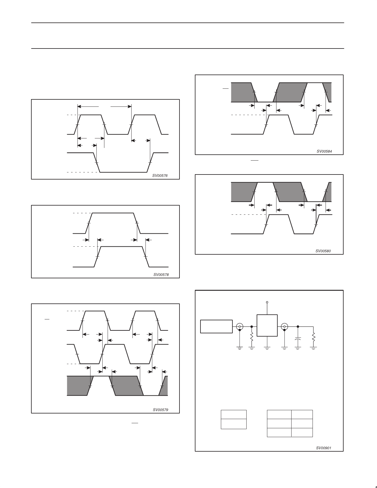
TEST CIRCUIT
VCC
PULSE
GENERATOR
VI
RT
D.U.T.
VO
50pF
CL
RL = 1KΩ
Test Circuit for switching times
DEFINITIONS
RL = Load resistor
CL = Load capacitance includes jig and probe capacitance
RT = Termination resistance should be equal to ZOUT
of pulse generators.
SWITCH POSITION
TEST
VCC
VI
tPLH/tPHL
< 2.7V VCC
2.7–3.6V 2.7V
SV00901
Figure 6. Load circuitry for switching times.
1998 Apr 30
9
Share Link: 