74ALVC16839 데이터 시트보기 (PDF) - Fairchild Semiconductor
부품명
상세내역
제조사
74ALVC16839
Fairchild Semiconductor
74ALVC16839 Datasheet PDF : 6 Pages
| |||
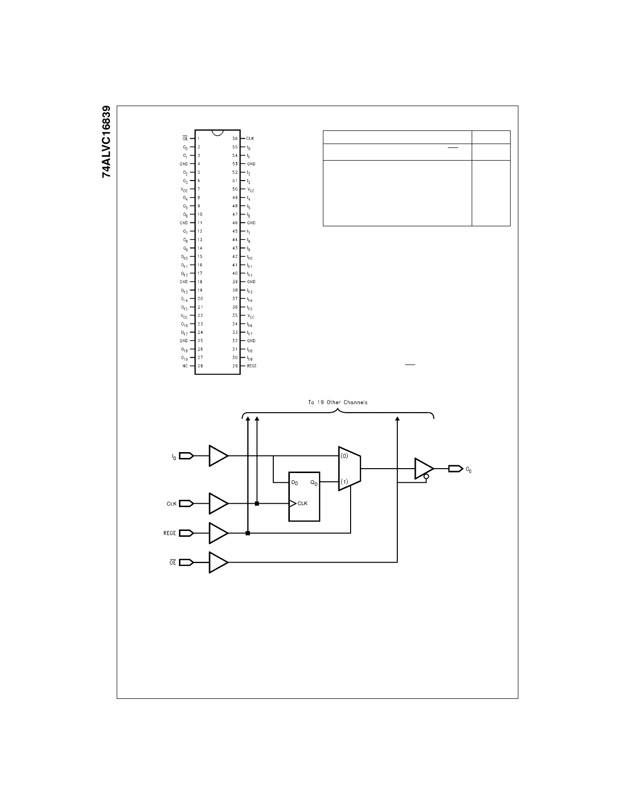
Connection Diagram
Logic Diagram
Truth Table
Inputs
Outputs
CLK
REGE
In
↑
H
H
↑
H
L
X
L
H
X
L
L
X
X
X
H = Logic HIGH
L = Logic LOW
X = Don’t Care, but not floating
Z = High Impedance
↑ = LOW-to-HIGH Clock Transition
OE
On
L
H
L
L
L
H
L
L
H
Z
Functional Description
The 74ALVC16839 consists of twenty selectable non-
inverting buffers or registers with word wide modes. Mode
functionality is selected through operation of the CLK and
REGE pin as shown by the truth table. When REGE is held
at a logic HIGH the device operates as a 20-bit register.
Data is transferred from In to On on the rising edge of the
CLK input. When the REGE pin is held at a logic LOW the
device operates in a flow through mode and data propa-
gates directly from the In to the On outputs. All outputs can
be 3-stated by holding the OE pin at a logic HIGH.
www.fairchildsemi.com
2
Share Link: 