AD9142A 데이터 시트보기 (PDF) - Analog Devices
부품명
상세내역
제조사
AD9142A Datasheet PDF : 72 Pages
| |||
Data Sheet
AD9142A
DAC LATENCY SPECIFICATIONS
TMIN to TMAX, AVDD33 = 3.3 V, DVDD18 = 1.8 V, CVDD18 = 1.8 V, IOUTFS = 20 mA, FIFO level is set to 4 (half of the FIFO depth), unless
otherwise noted.
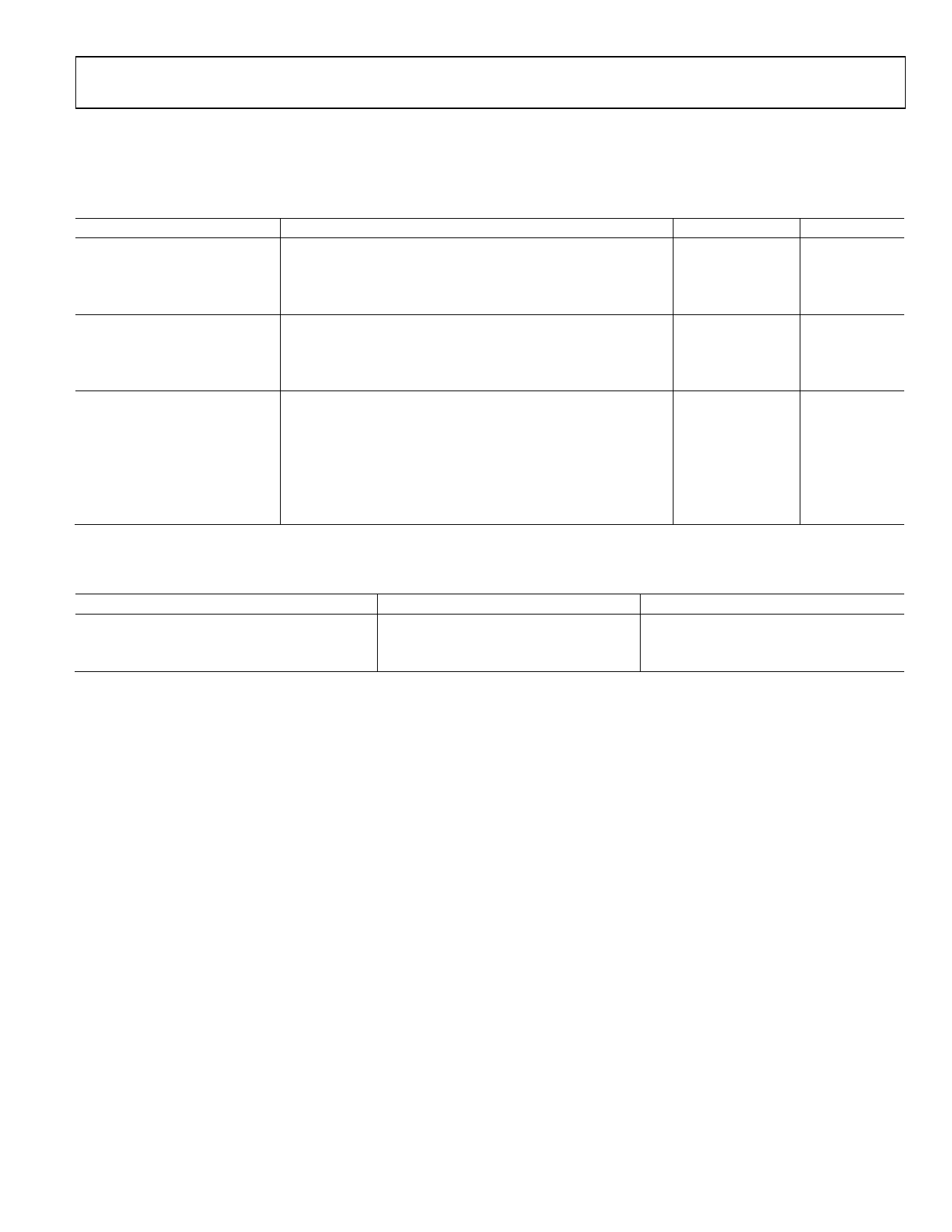
Table 3.
Parameter
WORD INTERFACE MODE
2× Interpolation
4× Interpolation
8× Interpolation
BYTE INTERFACE MODE
2× Interpolation
4× Interpolation
8× Interpolation
INDIVIDUAL FUNCTION BLOCKS
Modulation
Fine
Coarse
Inverse Sinc
Phase Compensation
Gain Compensation
Test Conditions/Comments
Fine/coarse modulation, inverse sinc, gain/phase compensation off
Fine/coarse modulation, inverse sinc, gain/phase compensation off
Min Typ Max Unit
134
DACCLK cycles
244
DACCLK cycles
481
DACCLK cycles
145
DACCLK cycles
271
DACCLK cycles
506
DACCLK cycles
17
DACCLK cycles
10
DACCLK cycles
20
DACCLK cycles
12
DACCLK cycles
16
DACCLK cycles
LATENCY VARIATION SPECIFICATIONS
Table 4.
Parameter
DAC LATENCY VARIATION1
SYNC Off
SYNC On
Min
Typ
Max
Unit
1
2
DACCLK cycles
0
1
DACCLK cycles
1 DAC latency is defined as the elapsed time from a data sample clocked at the input to the AD9142A until the analog output begins to change.
Rev. A | Page 9 of 72
Share Link: 