MAX19706ETM 데이터 시트보기 (PDF) - Maxim Integrated
부품명
상세내역
제조사
MAX19706ETM Datasheet PDF : 37 Pages
| |||
10-Bit, 22Msps, Ultra-Low-Power
Analog Front-End
ABSOLUTE MAXIMUM RATINGS
VDD to GND, OVDD to OGND ..............................-0.3V to +3.6V
GND to OGND.......................................................-0.3V to +0.3V
IAP, IAN, QAP, QAN, IDP, IDN, QDP,
QDN, DAC1, DAC2, DAC3 to GND......................-0.3V to VDD
ADC1, ADC2 to GND .................................-0.3V to (VDD + 0.3V)
REFP, REFN, REFIN, COM to GND ............-0.3V to (VDD + 0.3V)
D0–D9, DOUT, T/R, SHDN, SCLK, DIN, CS,
CLK to OGND ......................................-0.3V to (OVDD + 0.3V)
Continuous Power Dissipation (TA = +70°C)
48-Pin Thin QFN (derate 27.8mW/°C above +70°C) .....2.22W
Thermal Resistance θJA ..................................................36°C/W
Operating Temperature Range ...........................-40°C to +85°C
Junction Temperature ......................................................+150°C
Storage Temperature Range .............................-60°C to +150°C
Lead Temperature (soldering, 10s) .................................+300°C
Stresses beyond those listed under “Absolute Maximum Ratings” may cause permanent damage to the device. These are stress ratings only, and functional
operation of the device at these or any other conditions beyond those indicated in the operational sections of the specifications is not implied. Exposure to
absolute maximum rating conditions for extended periods may affect device reliability.
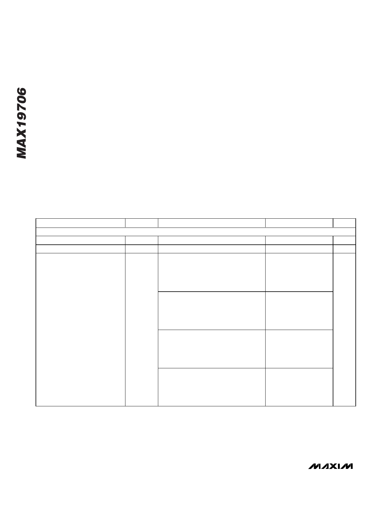
ELECTRICAL CHARACTERISTICS
(VDD = 3V, OVDD = 1.8V, internal reference (1.024V), CL ≈ 10pF on all digital outputs, fCLK = 22MHz (50% duty cycle), Rx ADC input
amplitude = -0.5dBFS, Tx DAC output amplitude = 0dBFS, differential Rx ADC input, differential Tx DAC output, CREFP = CREFN =
CCOM = 0.33µF, unless otherwise noted. CL < 5pF on all aux-DAC outputs. Typical values are at TA = +25°C.) (Note 1)
PARAMETER
POWER REQUIREMENTS
Analog Supply Voltage
Output Supply Voltage
SYMBOL
CONDITIONS
MIN TYP MAX UNITS
VDD
OVDD
2.7
3.0
3.3
V
1.8
VDD
V
Ext1-Tx, Ext3-Tx, and SPI2-Tx states;
transmit DAC operating mode (Tx):
fCLK = 22MHz, fOUT = 2.2MHz on both
11.3
channels; aux-DACs ON and at midscale,
aux-ADC ON
VDD Supply Current
Ext2-Tx, Ext4-Tx, and SPI4-Tx states;
transmit DAC operating mode (Tx):
fCLK = 22MHz, fOUT = 2.2MHz on both
channels; aux-DACs ON and at midscale,
aux-ADC ON
Ext1-Rx, Ext4-Rx, and SPI3-Rx states;
receive ADC operating mode (Rx):
fCLK = 22MHz, fIN = 5.5MHz on both
channels; aux-DACs ON and at midscale,
aux-ADC ON
16.5
20
mA
15.6
19
Ext2-Rx, Ext3-Rx, and SPI1-Rx states;
receive ADC operating mode (Rx):
fCLK = 22MHz, fIN = 5.5MHz on both
13.1
channels; aux-DACs ON and at midscale,
aux-ADC ON
2 _______________________________________________________________________________________
Share Link: 