M52347FP 데이터 시트보기 (PDF) - Renesas Electronics
부품명
상세내역
제조사
M52347FP Datasheet PDF : 17 Pages
| |||
M52347SP/FP
Pin Description
Pin No. Name
1
H.STATE
DC Voltage
(V)
0 VDC or
5 VDC
2
V.STATE
0 VDC or
5 VDC
3
CLAMP
2.2 V when
SW
open
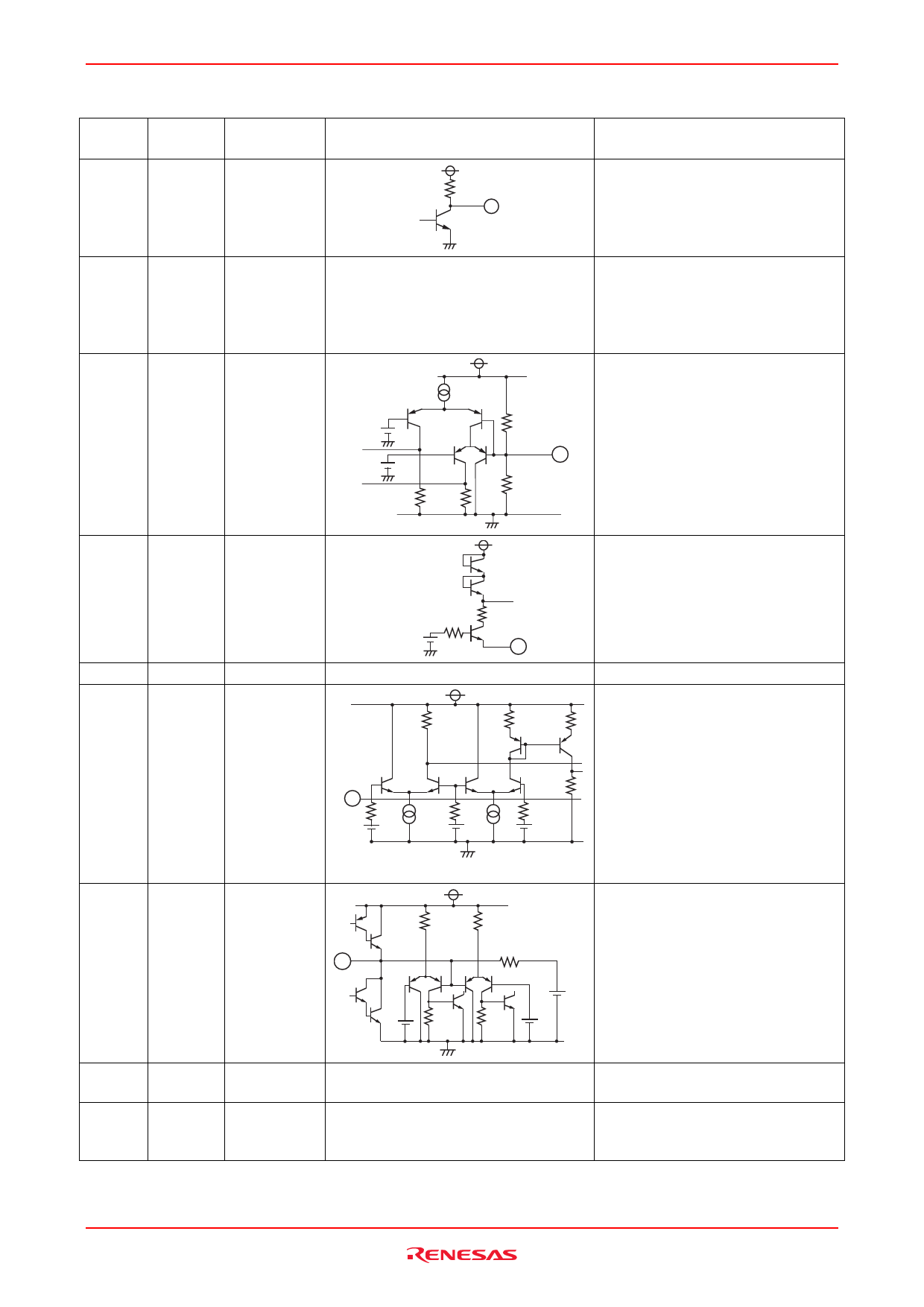
Peripheral Circuit
20 kΩ
1
Same as pin 1
0.1 mA
3.1 V
1.3 V
20 kΩ 20 kΩ
28 kΩ
3
22 kΩ
Function
Logic output pin for horizontal
synchronous signal
When pin 6 input signal is POSI,
outputs "H"; when NON, outputs "L";
and when NEG, outputs "H".
Logic output pin for vertical
synchronous signal
When pin 8 input signal is POSI,
outputs "H"; when NON, outputs "L";
and when NEG, outputs "H".
This SW is available to change the
generating position of clamp pulse for
input signal. (See Table 2.)
VTH L = 0 to 1 V
VTH M = 1.6 to 2.8 V
VTH H = 3.4 to 5 V
4
GREEN
2.8 V
IN
when open
3.5 V
1 kΩ 1 kΩ
4
GREEN (SYNC ON VIDEO) input pin
Input with negative sync.
Comparison of pin 4 input signal and
reference voltage within the IC
performs synchronous separation.
5
GND
Grounding
6
COMP/H
2.5 V
IN
when open
20 kΩ
1.5 kΩ
1.5 kΩ
Composite sync/H sync input pin.
Bias is approx. 2.5 V and impedance
is 10 kΩ.
6
10 kΩ
2.8 V
10 kΩ
2.5 V
0.3 mA
20 kΩ
0.3 mA
10 kΩ
2.2 V
The internal double threshold
comparator is used for shaping
waveform and detecting polarity.
Optimum input amplitude is 0.6 VP-P
at pin 6. Up to approx. 50% of duty,
waveform shaping and polarity
detection can be done.
7
COMP/H
2.5 V
External capacitance is required as a
DET
when open
(no signal)
12 kΩ 12 kΩ
filter pin for detecting polarity and
detecting non-input. As the value is
75 kΩ
larger, the ripple is smaller and less
7
malfunction occurs. However, this
2.5 V lowers the response speed of
2.8 V
20 kΩ
20 kΩ
2.2 V
detection.
8
V IN
9
V DET
2.5 V
when open
2.5 V
when open
(no signal)
Same as pin 6
Same as pin 7
V sync input pin
Same as pin 6
Same as pin 7
Rev.2.00 Sep 14, 2006 page 7 of 16
Share Link: 