AD2S44 데이터 시트보기 (PDF) - Analog Devices
부품명
상세내역
제조사
AD2S44 Datasheet PDF : 12 Pages
| |||
AD2S44
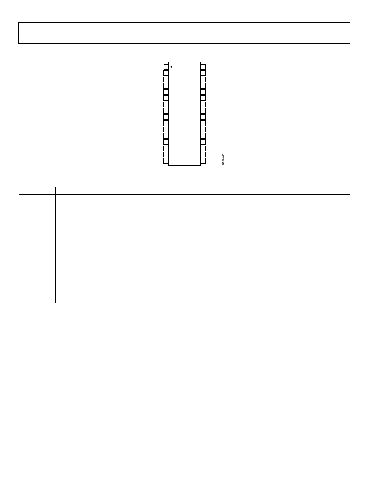
PIN CONFIGURATION AND FUNCTION DESCRIPTIONS
DB8 1
DB9 2
DB10 3
DB11 4
DB12 5
DB13 6
DB14 (LSB) 7
OE 8
A/B 9
BIT 10
RLO (A) 11
RHI (A) 12
S4 (A) 13
S3 (A) 14
S2 (A) 15
S1 (A) 16
AD2S44
TOP VIEW
(Not to Scale)
32 DB7
31 DB6
30 DB5
29 DB4
28 DB3
27 DB2
26 DB1 (MSB)
25 +VS
24 –VS
23 GND
22 RLO (B)
21 RHI (B)
20 S4 (B)
19 S3 (B)
18 S2 (B)
17 S1 (B)
Figure 2. Pin Configuration
Table 3. Pin Function Descriptions
Pin No.
Mnemonic
1 to 7
DB8 to DB14 (LSB)
8
OE
9
A/B
10
BIT
11
RLO (A)
12
RHI (A)
13 to 16
S4 (A) to S1 (A)
17 to 20
S1 (B) to S4 (B)
21
RHI (B)
22
RLO (B)
23
GND
24
–VS
25
+VS
26 to 32
DB1 (MSB) to DB7
Description
Parallel Output Data Bits.
Output Enable Input.
Channel A or Channel B Select Input.
Built-In Test Error Output.
Input Pin for Channel A Reference Low.
Input Pin for Channel A Reference High.
Channel A Input Signal.
Channel B Input Signal.
Input Pin for Channel B Reference High.
Input Pin for Channel B Reference Low.
Power Supply Ground. This pin is electrically connected to the case.
Negative Power Supply.
Positive Power Supply.
Parallel Output Data Bits.
Data Sheet
Rev. B | Page 6 of 12
Share Link: 