CY7C1486BV25-250BGI 데이터 시트보기 (PDF) - Cypress Semiconductor
부품명
상세내역
제조사
CY7C1486BV25-250BGI Datasheet PDF : 31 Pages
| |||
CY7C1480BV25
CY7C1482BV25, CY7C1486BV25
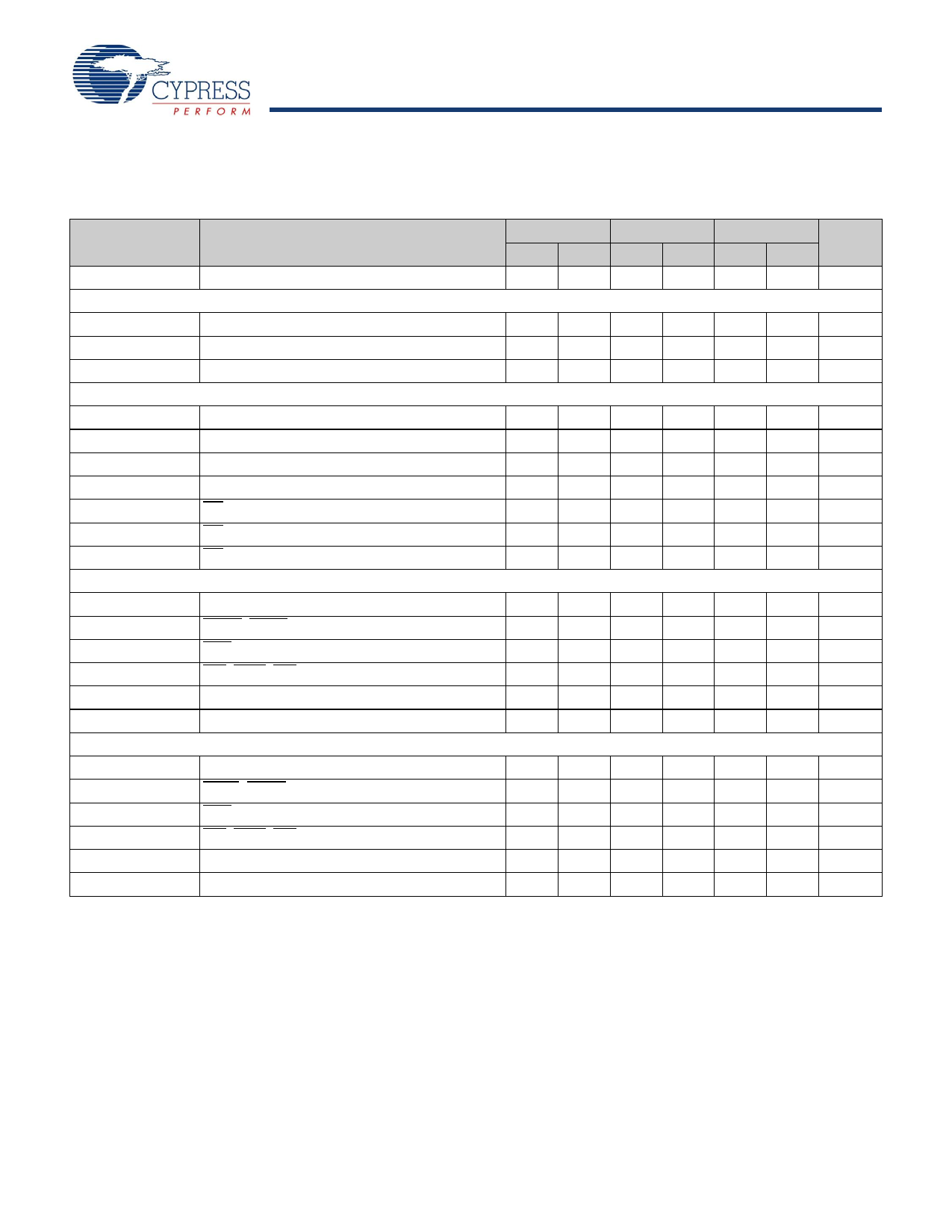
Switching Characteristics
Over the Operating Range. Timing reference level is 1.25V when VDDQ = 2.5V. Test conditions shown in (a) of “AC Test Loads and
Waveforms” on page 20 unless otherwise noted.
Parameter
tPOWER
Clock
tCYC
tCH
tCL
Output Times
tCO
tDOH
tCLZ
tCHZ
tOEV
tOELZ
tOEHZ
Setup Times
tAS
tADS
tADVS
tWES
tDS
tCES
Hold Times
tAH
tADH
tADVH
tWEH
tDH
tCEH
Description
VDD(Typical) to the first access[15]
Clock Cycle Time
Clock HIGH
Clock LOW
Data Output Valid After CLK Rise
Data Output Hold After CLK Rise
Clock to Low-Z[16, 17, 18]
Clock to High-Z[16, 17, 18]
OE LOW to Output Valid
OE LOW to Output Low-Z[16, 17, 18]
OE HIGH to Output High-Z[16, 17, 18]
Address Setup Before CLK Rise
ADSC, ADSP Setup Before CLK Rise
ADV Setup Before CLK Rise
GW, BWE, BWX Setup Before CLK Rise
Data Input Setup Before CLK Rise
Chip Enable Setup Before CLK Rise
Address Hold After CLK Rise
ADSP, ADSC Hold After CLK Rise
ADV Hold After CLK Rise
GW, BWE, BWX Hold After CLK Rise
Data Input Hold After CLK Rise
Chip Enable Hold After CLK Rise
250 MHz
200 MHz
167 MHz
Unit
Min Max Min Max Min Max
1
1
1
ms
4.0
5.0
6.0
ns
2.0
2.0
2.4
ns
2.0
2.0
2.4
ns
3.0
3.0
3.4
ns
1.3
1.3
1.5
ns
1.3
1.3
1.5
ns
3.0
3.0
3.4
ns
3.0
3.0
3.4
ns
0
0
0
ns
3.0
3.0
3.4
ns
1.4
1.4
1.5
ns
1.4
1.4
1.5
ns
1.4
1.4
1.5
ns
1.4
1.4
1.5
ns
1.4
1.4
1.5
ns
1.4
1.4
1.5
ns
0.4
0.4
0.5
ns
0.4
0.4
0.5
ns
0.4
0.4
0.5
ns
0.4
0.4
0.5
ns
0.4
0.4
0.5
ns
0.4
0.4
0.5
ns
Notes
15. This part has an internal voltage regulator; tPOWER is the time that the power is supplied above VDD(minimum) initially before a read or write operation can be initiated.
16. tCHZ, tCLZ, tOELZ, and tOEHZ are specified with AC test conditions shown in part (b) of “AC Test Loads and Waveforms” on page 20. Transition is measured ±200 mV
from steady-state voltage.
17. At any possible voltage and temperature, tOEHZ is less than tOELZ and tCHZ is less than tCLZ to eliminate bus contention between SRAMs when sharing the same data
bus. These specifications do not imply a bus contention condition, but reflect parameters guaranteed over worst case user conditions. Device is designed to achieve
High-Z before Low-Z under the same system conditions.
18. This parameter is sampled and not 100% tested.
Document #: 001-15143 Rev. *D
Page 21 of 31
[+] Feedback
Share Link: 