MT47H128M8SH-25EITH 데이터 시트보기 (PDF) - Micron Technology
부품명
상세내역
제조사
MT47H128M8SH-25EITH Datasheet PDF : 133 Pages
| |||
FBGA Package Capacitance
1Gb: x4, x8, x16 DDR2 SDRAM
Packaging
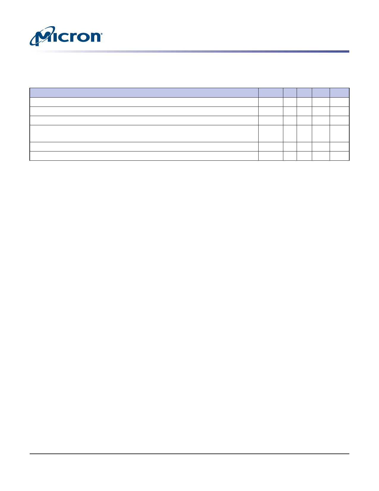
Table 4: Input Capacitance
Parameter
Symbol Min Max Units Notes
Input capacitance: CK, CK#
CCK 1.0 2.0 pF
1
Delta input capacitance: CK, CK#
CDCK – 0.25 pF 2, 3
Input capacitance: Address balls, bank address balls, CS#, RAS#, CAS#, WE#, CKE, ODT
CI
1.0 2.0 pF 1, 4
Delta input capacitance: Address balls, bank address balls, CS#, RAS#, CAS#, WE#, CKE, CDI
ODT
– 0.25 pF 2, 3
Input/output capacitance: DQ, DQS, DM, NF
Delta input/output capacitance: DQ, DQS, DM, NF
CIO 2.5 4.0 pF 1, 5
CDIO
– 0.5 pF 2, 3
Notes:
1. This parameter is sampled. VDD = 1.8V ±0.1V, VDDQ = 1.8V ±0.1V, VREF = VSS, f = 100 MHz,
TC = 25°C, VOUT(DC) = VDDQ/2, VOUT (peak-to-peak) = 0.1V. DM input is grouped with I/O
balls, reflecting the fact that they are matched in loading.
2. The capacitance per ball group will not differ by more than this maximum amount for
any given device.
3. ΔC are not pass/fail parameters; they are targets.
4. Reduce MAX limit by 0.25pF for -25, -25E, and -187E speed devices.
5. Reduce MAX limit by 0.5pF for -3, -3E, -25, -25E, and -187E speed devices.
PDF: 09005aef8565148a
1GbDDR2.pdf – Rev. AA 07/14 EN
22
Micron Technology, Inc. reserves the right to change products or specifications without notice.
© 2007 Micron Technology, Inc. All rights reserved.
Share Link: 