MAX9234(2005) 데이터 시트보기 (PDF) - Maxim Integrated
부품명
상세내역
제조사
MAX9234 Datasheet PDF : 14 Pages
| |||
Hot-Swappable, 21-Bit, DC-Balanced LVDS
Deserializers
Power-Supply Bypassing
There are separate on-chip power domains for digital
circuits, outputs, PLL, and LVDS inputs. Bypass each
VCC, VCCO, PLL VCC, and LVDS VCC pin with high-fre-
quency, surface-mount ceramic 0.1µF and 0.001µF
capacitors in parallel as close to the device as possi-
ble, with the smallest value capacitor closest to the
supply pin.
Cables and Connectors
Interconnect for LVDS typically has a differential imped-
ance of 100Ω. Use cables and connectors that have
matched differential impedance to minimize impedance
discontinuities.
Twisted-pair and shielded twisted-pair cables offer
superior signal quality compared to ribbon cable and
tend to generate less EMI due to magnetic field cancel-
ing effects. Balanced cables pick up noise as common
mode, which is rejected by the LVDS receiver.
Board Layout
Keep the LVTTL/LVCMOS outputs and LVDS input sig-
nals separated to prevent crosstalk. A four-layer PC
board with separate layers for power, ground, LVDS
inputs, and digital signals is recommended.
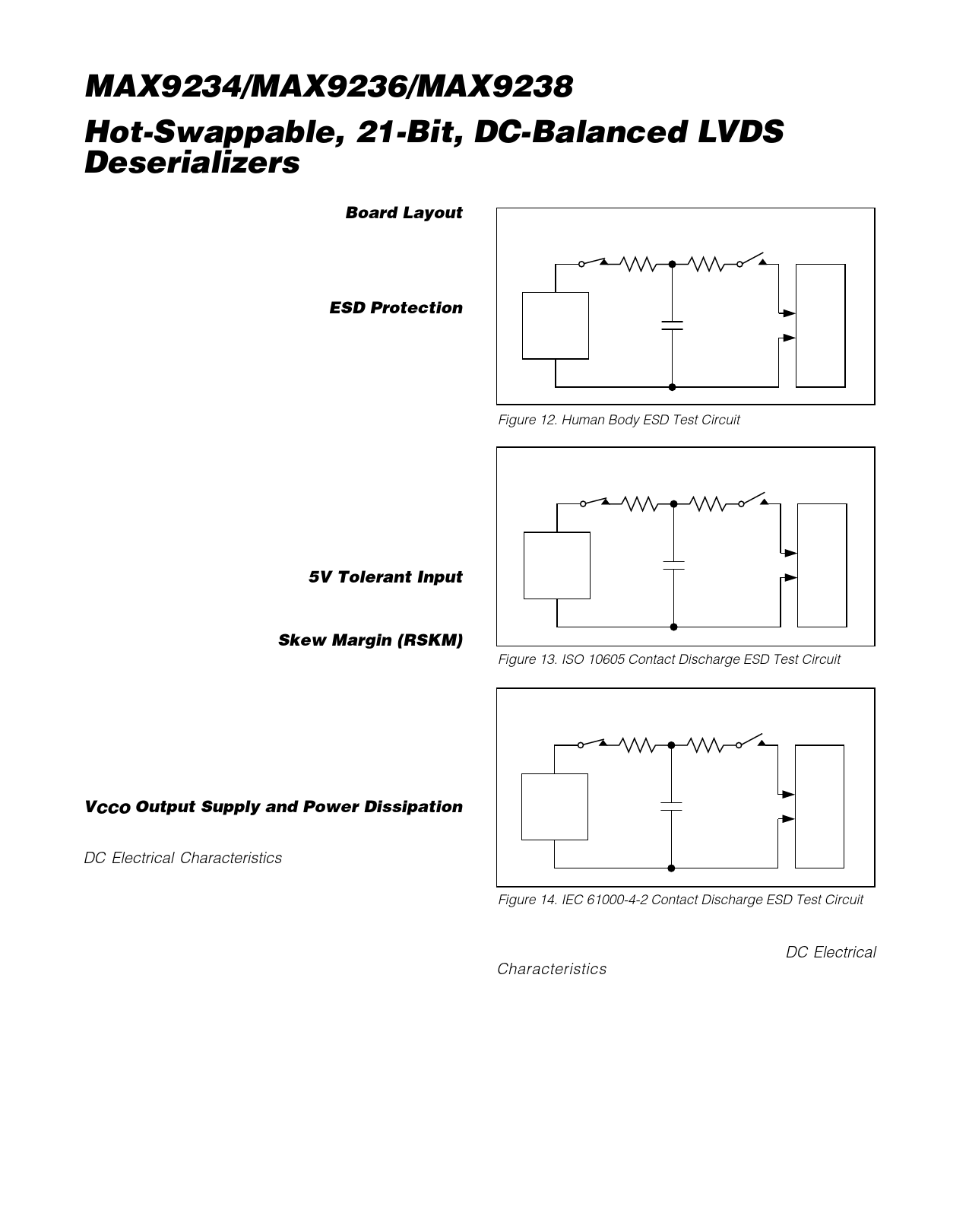
ESD Protection
The MAX9234/MAX9236/MAX9238 ESD tolerance is
rated for Human Body Model and ISO 10605 standards.
ISO 10605 specifies ESD tolerance for electronic sys-
tems. The Human Body Model discharge components
are CS = 100pF and RD = 1.5kΩ (Figure 12). For the
Human Body Model, all pins are rated for ±5kV contact
discharge. The ISO 10605 discharge components are
CS = 330pF and RD = 2kΩ (Figure 13). For ISO 10605,
the LVDS outputs are rated for ±8kV contact and ±25kV
air discharge.
5V Tolerant Input
PWRDWN is 5V tolerant and is internally pulled down to
GND.
Skew Margin (RSKM)
Skew margin (RSKM) is the time allowed for degrada-
tion of the serial data sampling setup and hold times by
sources other than the deserializer. The deserializer
sampling uncertainty is accounted for and does not
need to be subtracted from RSKM. The main outside
contributors of jitter and skew that subtract from RSKM
are interconnect intersymbol interference, serializer
pulse position uncertainty, and pair-to-pair path skew.
VCCO Output Supply and Power Dissipation
The outputs have a separate supply (VCCO) for interfacing
to systems with 1.8V to 5V nominal input-logic levels. The
DC Electrical Characteristics table gives the maximum
supply current for VCCO = 3.6V with 8pF load at several
switching frequencies with all outputs switching in the
worst-case switching pattern. The approximate incremen-
tal supply current for VCCO other than 3.6V with the same
8pF load and worst-case pattern can be calculated using:
II = CTVI 0.5fC x 21 (data outputs)
+ CTVIfC x 1 (clock output)
where:
II = incremental supply current.
CT = total internal (CINT) and external (CL) load capaci-
tance.
VI = incremental supply voltage.
fC = output clock-switching frequency.
The incremental current is added to (for VCCO > 3.6V)
or subtracted from (for VCCO < 3.6V) the DC Electrical
Characteristics table maximum supply current. The
internal output buffer capacitance is CINT = 6pF. The
worst-case pattern-switching frequency of the data out-
puts is half the switching frequency of the output clock.
R1
R2
1MΩ
1.5kΩ
HIGH-
VOLTAGE
DC
SOURCE
CHARGE-CURRENT-
LIMIT RESISTOR
CS
100pF
DISCHARGE
RESISTANCE
STORAGE
CAPACITOR
DEVICE
UNDER
TEST
R1
R2
50Ω TO 100Ω
2kΩ
HIGH-
VOLTAGE
DC
SOURCE
CHARGE-CURRENT-
LIMIT RESISTOR
CS
330pF
DISCHARGE
RESISTANCE
STORAGE
CAPACITOR
DEVICE
UNDER
TEST
Figure 12. Human Body ESD Test Circuit
Figure 13. ISO 10605 Contact Discharge ESD Test Circuit
12 ______________________________________________________________________________________
Share Link: 