BU941 데이터 시트보기 (PDF) - Unisonic Technologies
부품명
상세내역
제조사
BU941 Datasheet PDF : 5 Pages
| |||
BU941
NPN SILICON TRANSISTOR
ABSOLUTE MAXIMUM RATINGS
PARAMETER
SYMBOL
RATINGS
UNIT
Collector-Emitter Voltage
VCES
500
V
Collector-Emitter Voltage
VCEO
400
V
Emitter-Base Voltage
VEBO
5
V
Collector Current
IC
15
A
Collector Peak Current
ICM
30
A
Base Current
IB
1
A
Base Peak Current
IBM
5
W
TO-3P
155
W
Total Power Dissipation (Tc=25°C)
TO-220
PD
150
W
TO-263
65
W
Junction Temperature
Storage Temperature
TJ
+175
°C
TSTG
-65 ~ +175
°C
Note Absolute maximum ratings are those values beyond which the device could be permanently damaged.
Absolute maximum ratings are stress ratings only and functional device operation is not implied.
ELECTRICAL CHARACTERISTICS (Tc=25°C, unless otherwise specified)
PARAMETER
SYMBOL
TEST CONDITIONS
MIN TYP MAX UNIT
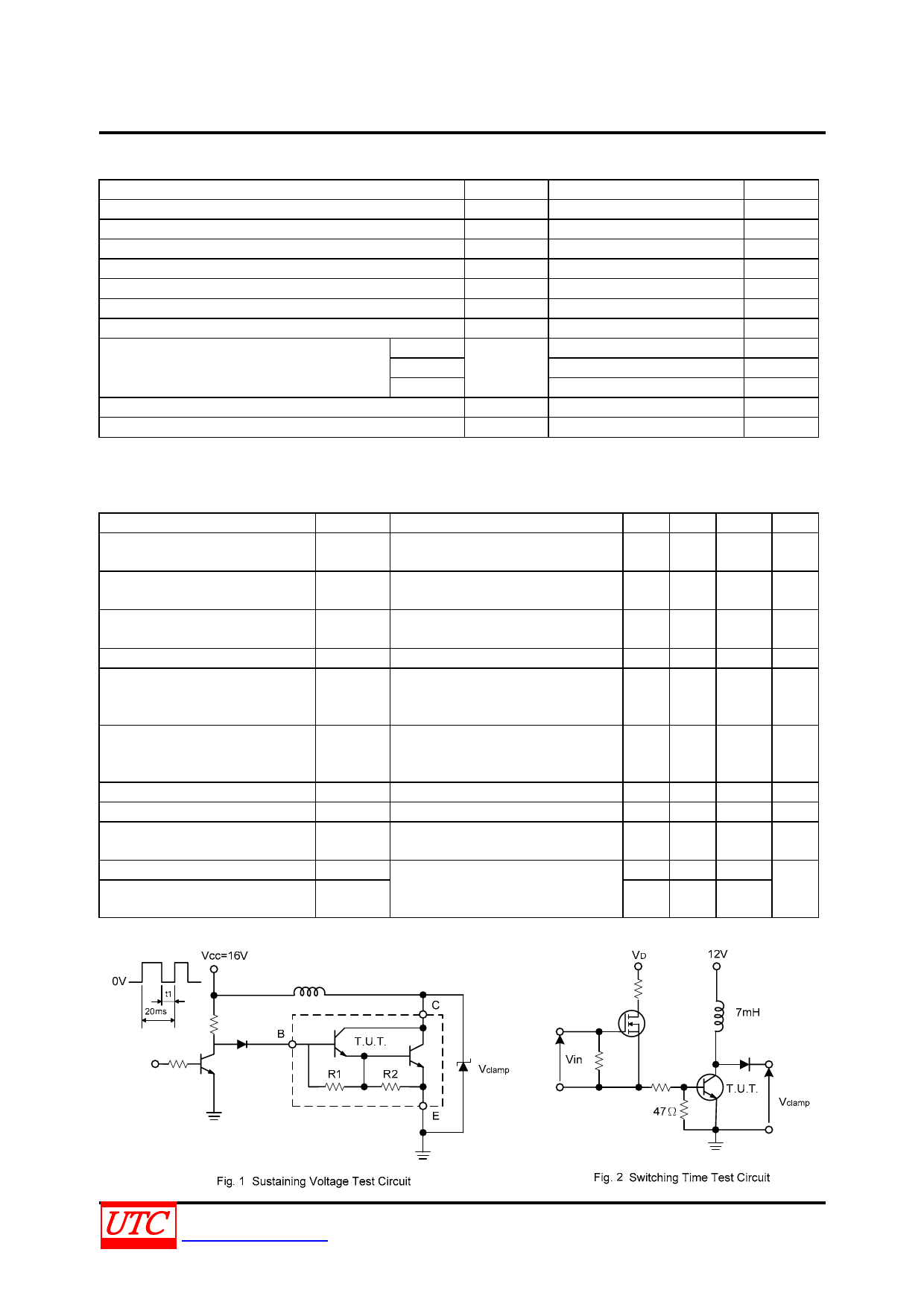
Collector-Emitter Sustaining
Ic=100mA, Vclamp=400V, L=10mH
Voltage
VCEO(SUS)* (see Fig. 1)
400
V
Collector Cut-Off Current
ICES
VCE=500V, VBE=0
VCE=500V, VBE=0, TJ=125°C
100 µA
0.5 mA
Collector Cut-Off Current
ICEO
VCE=450V, IB=0
VCE=450V, IB=0, TJ=125°C
100 µA
0.5 mA
Emitter Cut-off Current
IEBO VEB=5V, Ic=0
20 mA
Collector-Emitter Saturation
Voltage
IC=8A, IB=100mA
VCE(SAT)* IC=10A, IB=250mA
IC=12A, IB=300mA
1.6
1.8
V
2
Base-Emitter Saturation Voltage
IC=8A, IB=100mA
VBE(SAT)* IC=10A, IB=250mA
IC=12A, IB=300mA
2.2
2.5
V
2.7
DC Current Gain
hFE* VCE=10V, Ic=5A
300
Diode Forward Voltage
VF
IF=10A
2.5
V
Functional Test
VCC=24V, Vclamp=400V, L=7mH
10
A
(see Functional Test Circuit)
Fall Time
Storage Time
tF
VCC=12V, Vclamp=300V, VBE=0,
15
ts
RBE=47Ω, L=7mH, Ic=7A, IB=70mA
(see Fig.2)
0.5
µs
*Pulsed: Pulse duration=300µs, duty cycle 1.5%
UNISONIC TECHNOLOGIES CO., LTD
www.unisonic.com.tw
2 of 5
QW-R203-025,B
Share Link: 