G547F1P11U 데이터 시트보기 (PDF) - Unspecified
부품명
상세내역
제조사
G547F1P11U Datasheet PDF : 15 Pages
| |||
Global Mixed-mode Technology
Pin Description
G547E/F/G/H/M
SOT-23-6
2
3
1
6
4,5
PIN
SOP-8/MSOP-8 TDFN3X3-8
1
1
2,3
2,3
4
5
6,7,8
4
5
6,7,8
Thermal Pad
NAME
GND
IN
EN( EN )
OC
OUT
PIN FUNCTION
Ground
Input Supply: Output MOSFET Drain, which also supplies IC's in-
ternal circuitry. Connect to positive supply.
Enable: Logic level enable input.
Make sure EN pin never floating.
Over-Current: Open-Drain OC output.
Switch Output: Output MOSFET Source of switch. Typically connect
to switched side of load.
Recommend connecting the Thermal Pad to the GND for excellent
power dissipation.
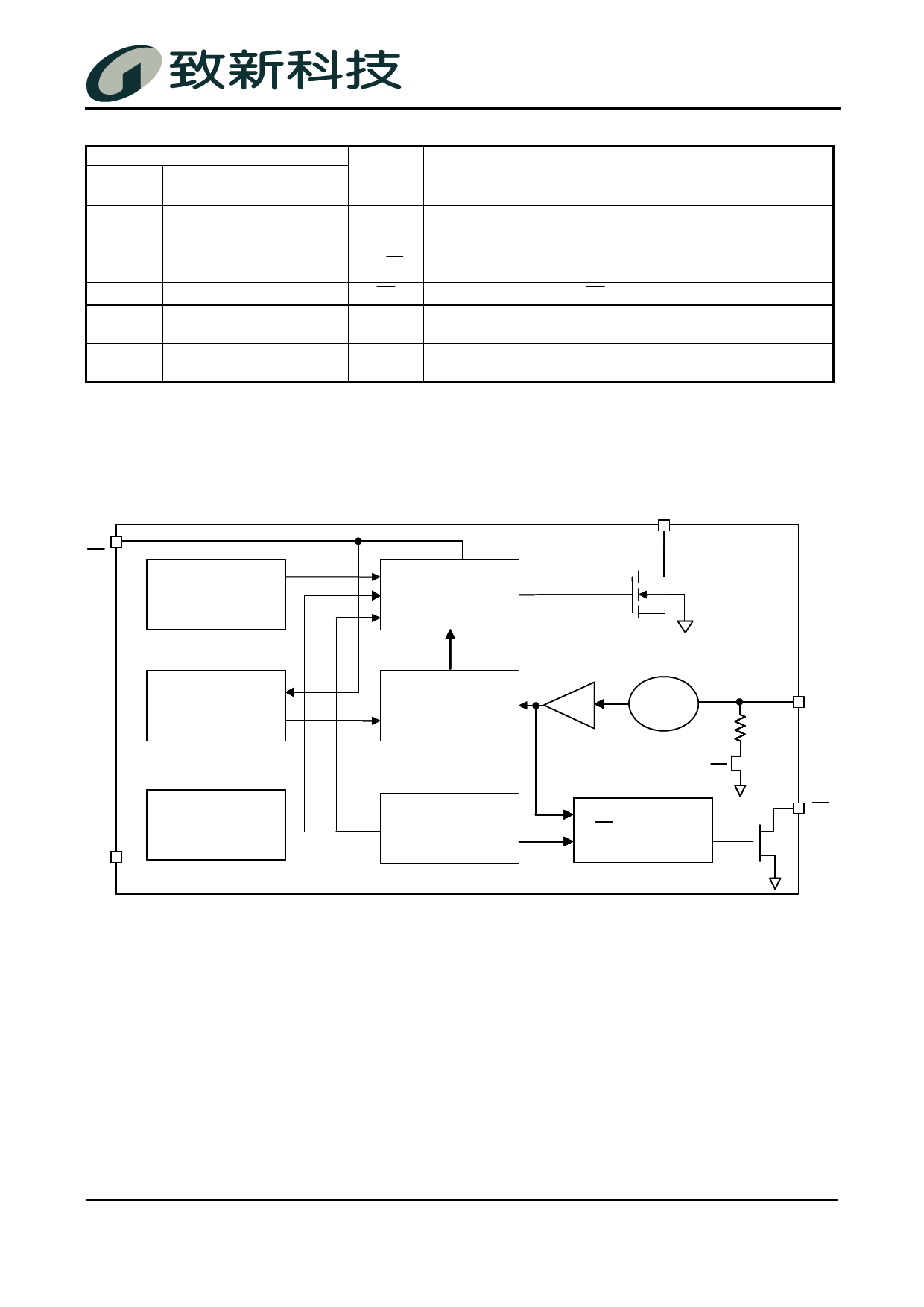
Block Diagram
IN
EN
(EN)
Clock
BandGap
Reference
技 Gate Control
海恒通t科ech.com Overcurrent
w四ww.gofo Limiting
CMP
Current
Sense
Shutdown Signal
OUT
OC
UVLO
Thermal Sense
OC Deglitch logic
GND
Ver:1.5
Sep 08, 2011
9
Share Link: 