M30201F4-XXXSP 데이터 시트보기 (PDF) - MITSUBISHI ELECTRIC
부품명
상세내역
제조사
M30201F4-XXXSP Datasheet PDF : 159 Pages
| |||
Clock Generating Circuit
Mitsubishi microcomputers
M30201 Group
SINGLE-CHIP 16-BIT CMOS MICROCOMPUTER
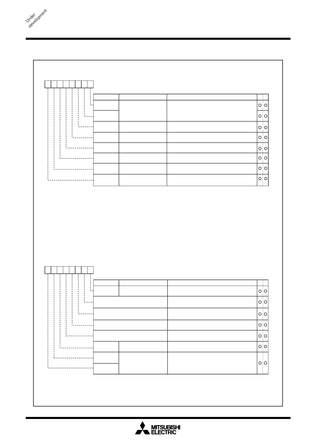
Figure 1.18 shows the system clock control registers 0 and 1.
System clock control register 0 (Note 1)
b7 b6 b5 b4 b3 b2 b1 b0
Symbol
CM0
Address
000616
When reset
4816
Bit symbol
CM00
CM01
CM02
CM03
CM04
CM05
CM06
CM07
Bit name
Clock output function
select bit
WAIT peripheral function
clock stop bit
Function
b1 b0
0 0 : I/O port P54
0 1 : fC output
1 0 : f8 output
1 1 : Clock divide counter output
0 : Do not stop peripheral function clock in wait mode
1 : Stop peripheral function clock in wait mode (Note 8)
XCIN-XCOUT drive capacity 0 : LOW
select bit (Note 2)
1 : HIGH
Port XC select bit
Main clock (XIN-XOUT)
stop bit (Note 3,4,5)
0 : I/O port
1 : XCIN-XCOUT generation
0 : On
1 : Off
Main clock division select 0 : CM16 and CM17 valid
bit 0 (Note 7)
1 : Division by 8 mode
System clock select bit
(Note 6)
0 : XIN, XOUT
1 : XCIN, XCOUT
RW
Note 1: Set bit 0 of the protect register (address 000A16) to “1” before writing to this register.
Note 2: Changes to “1” when shifting to stop mode and at a reset.
Note 3: This bit is used to stop the main clock when placing the device in a low-power mode. If you want to operate with XIN
after exiting from the stop mode, set this bit to “0”. When operating with a self-excited oscillator, set the system clock
select bit (CM07) to “1” before setting this bit to “1”.
Note 4: When inputting external clock, only clock oscillation buffer is stopped and clock input is acceptable.
Note 5: If this bit is set to “1”, XOUT turns “H”. The built-in feedback resistor remains being connected, so XIN turns pulled up to
XOUT (“H”) via the feedback resistor.
Note 6: Set port Xc select bit (CM04) to “1” and stabilize the sub-clock oscillating before setting to this bit from “0” to “1”.
Do not write to both bits at the same time. And also, set the main clock stop bit (CM05) to “0” and stabilize the main clock
oscillating before setting this bit from “1” to “0”.
Note 7: This bit changes to “1” when shifting from high-speed/medium-speed mode to stop mode and at a reset. When shifting
from low-speed/low power dissipation mode to stop mode, the value before stop mode is retained.
Note 8: fC32 is not included.
System clock control register 1 (Note 1)
b7 b6 b5 b4 b3 b2 b1 b0
0 00 0
Symbol
CM1
Address
000716
When reset
2016
Bit symbol
Bit name
CM10
All clock stop control bit
(Note 4)
Reserved bit
Function
0 : Clock on
1 : All clocks off (stop mode)
Always set to “0”
RW
Reserved bit
Always set to “0”
Reserved bit
Always set to “0”
Reserved bit
Always set to “0”
CM15
CM16
CM17
XIN-XOUT drive capacity
select bit (Note 2)
Main clock division
select bit 1 (Note 3)
0 : LOW
1 : HIGH
b7 b6
0 0 : No division mode
0 1 : Division by 2 mode
1 0 : Division by 4 mode
1 1 : Division by 16 mode
Note 1: Set bit 0 of the protect register (address 000A16) to “1” before writing to this register.
Note 2: This bit changes to “1” when shifting from high-speed/medium-speed mode to stop mode and at a reset. When shifting
from low-speed/low power dissipation mode to stop mode, the value before stop mode is retained.
Note 3: Can be selected when bit 6 of the system clock control register 0 (address 000616) is “0”. If “1”, division mode is fixed at 8.
Note 4: If this bit is set to “1”, XOUT turns “H”, and the built-in feedback resistor is cut off. XCIN and XCOUT turn high-impedance state.
Figure 1.18. Clock control registers 0 and 1
21
Share Link: 