MC145170P2 데이터 시트보기 (PDF) - Motorola => Freescale
부품명
상세내역
제조사
MC145170P2 Datasheet PDF : 32 Pages
| |||
Pin Connections
Freescale Semiconductor, Inc.
3 Pin Connections
3.1 Digital Interface Pins
Din
Serial Data Input (Pin 5)
The bit stream begins with the most significant bit (MSB) and is shifted in on the low-to-high transition of
CLK. The bit pattern is 1 byte (8 bits) long to access the C or configuration register, 2 bytes (16 bits) to
access the N register, or 3 bytes (24 bits) to access the R register. Additionally, the R register can be
accessed with a 15-bit transfer (see Table 7). An optional pattern which resets the device is shown in
Figure 15. The values in the C, N, and R registers do not change during shifting because the transfer of
data to the registers is controlled by ENB.
The bit stream needs neither address nor steering bits due to the innovative BitGrabber registers.
Therefore, all bits in the stream are available to be data for the three registers. Random access of any
register is provided (i.e., the registers may be accessed in any sequence). Data is retained in the registers
over a supply range of 2.7 to 5.5 V. The formats are shown in Figures 15, 16, 17, and 18.
Din typically switches near 50% of VDD to maximize noise immunity. This input can be directly interfaced
to CMOS devices with outputs guaranteed to switch near rail-to-rail. When interfacing to NMOS or TTL
devices, either a level shifter (MC74HC14A, MC14504B) or pull-up resistor of 1 to 10 kΩ must be used.
Parameters to consider when sizing the resistor are worst-case IOL of the driving device, maximum
tolerable power consumption, and maximum data rate.
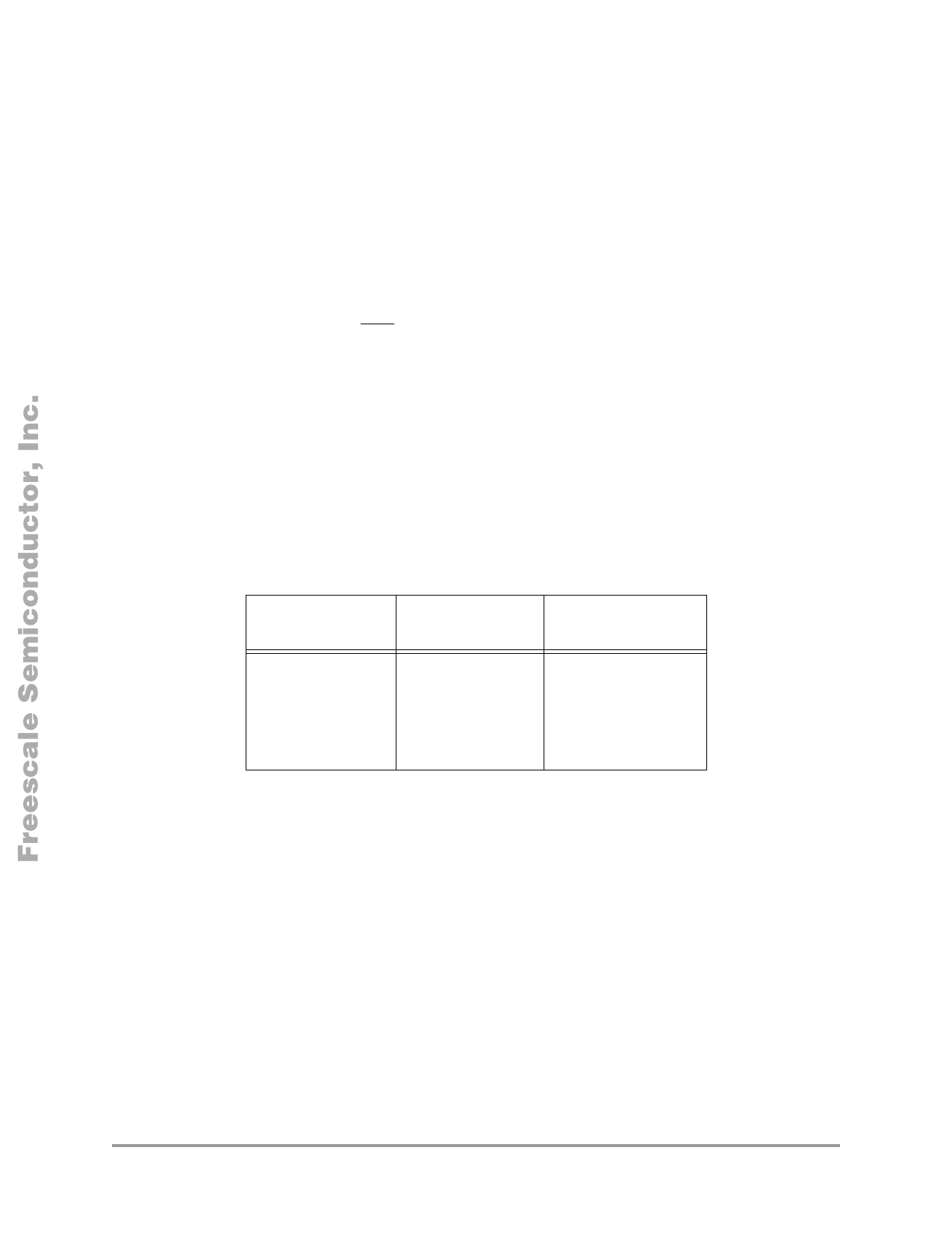
Table 7. Register Access
(MSBs are shifted in first, C0, N0, and R0 are the LSBs)
Number
of Clocks
Accessed
Register
Bit
Nomenclature
9 to 13
8
16
15 or 24
Other Values ≤ 32
Values > 32
See Figure 15
C Register
N Register
R Register
None
See Figures 27 to 34
(Reset)
C7, C6, C5, ..., C0
N15, N14, N13, ..., N0
R14, R13, R12, ..., R0
CLK
Serial Data Clock Input (Pin 7)
Low-to-high transitions on Clock shift bits available at Din, while high-to-low transitions shift bits from
Dout. The chip's 16-1/2-stage shift register is static, allowing clock rates down to dc in a continuous or
intermittent mode.
Four to eight clock cycles followed by five clock cycles are needed to reset the device; this is optional.
Eight clock cycles are required to access the C register. Sixteen clock cycles are needed for the N register.
Either 15 or 24 cycles can be used to access the R register (see Table 7 and Figures 15, 16, 17, and 18). For
cascaded devices, see Figures 27 to 34.
CLK typically switches near 50% of VDD and has a Schmitt-triggered input buffer. Slow CLK rise and fall
times are allowed. See the last paragraph of Din for more information.
NOTE: To guarantee proper operation of the power-on reset (POR) circuit, the CLK pin must be held at
the potential of either the VSS or VDD pin during power up. That is, the CLK input should not be floated or
toggled while the VDD pin is ramping from 0 to at least 2.7 V. If control of the CLK pin is not practical
during power up, the initialization sequence shown in Figure 15 must be used.
10
MC145170-2 Technical Data
MOTOROLA
For More Information On This Product,
Go to: www.freescale.com
Share Link: 