LTC7000MPMSE-1-PBF データシートの表示(PDF) - Analog Devices
部品番号
コンポーネント説明
メーカー
LTC7000MPMSE-1-PBF Datasheet PDF : 30 Pages
| |||
LTC7000/LTC7000-1
APPLICATIONS INFORMATION
Where 3.5V < Rising VCC UVLO < 10.5V.
11
10
9
8
7
6
5
4
3
2
1
RISING VCC UVLO
FALLING VCC UVLO
0
0 30 60 90 120 150 180 210 240
VCCUV RESISTOR TO GROUND (kΩ)
7000 F11
Figure 11. VCCUV Resistor Selection
MOSFET Selection
The most important parameters in high voltage applica-
tions for MOSFET selection are the breakdown voltage
BVDSS, on-resistance RDS(ON) and the safe operating area,
SOA.
The MOSFET, when off, will see the full input range of the
input power supply plus any additional ringing than can
occur when driving inductive loads.
External conduction losses are minimized when using low
RDS(ON) MOSFETs. Since many high voltage MOSFETs
have higher threshold voltages (typical VTH ≥ 5V) and
RDS(ON) is directly related to the (VGS–VTH) of the MOSFET,
the LTC7000/LTC7000-1 maximum gate drive of greater
than 10V makes it an ideal solution to minimize external
conduction losses associated with external high voltage
MOSFETs.
SOA is specified in Typical Characteristic curves in power
N-channel MOSFET data sheets. The SOA curves show
the relationship between the voltages and current allowed
in a timed operation of a power MOSFET without causing
damage to the MOSFET. The overcurrent trip point (RSNS
and RISET) of the LTC7000/LTC7000-1 and TIMER capaci-
tor should be chosen to stay within the SOA region of the
MOSFET selected for the application.
Limiting Inrush Current During Turn-On
Driving large capacitive loads such as complex electrical
systems with large bypass capacitors should be powered
using the circuit shown in Figure 12. The pull-up gate
drive to the power MOSFET from TGUP is passed through
an RC delay network, RG and CG, which greatly reduces
the turn-on ramp rate of the MOSFET. Since the MOSFET
source voltage follows the gate voltage, the load is pow-
ered smoothly from ground. This dramatically reduces
the inrush current from the source supply and reduces
the transient ramp rate of the load allowing for slower
activation of sensitive electrical loads. The turn-off of the
MOSFET is not affected by the RC delay network as the
pull-down for the MOSFET gate is directly from the TGDN
pin. Note that the voltage rating on capacitor CG needs
to be the same or higher than the external MOSFET and
CLOAD.
Adding CG to the gate of the external MOSFET can cause
high frequency oscillation. A low power, low ohmic value
resistor (10Ω) should be placed in series with CG to
dampen the oscillations as shown in Figure 12 whenever
CG is used in an application. Alternatively, the low ohmic
value resistor can be placed in series with the gate of the
external MOSFET.
LTC7000/
LTC7000-1
SNS+
SNS–
TGUP
TGDN
BST
TS
7000 F12
RFLT
RG 100k
VIN
RSNS
10Ω
CB
CG
0.047µF
1µF
LOAD
CLOAD
100µF
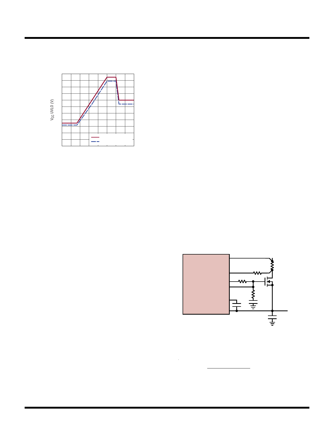
Figure 12. Powering Large Capacitive Loads
The values for RG and CG to limit the inrush current can
be calculated from the below equation:
IIN _ RUSH
≅
0.7
• 12V
RG •
• CLOAD
CG
For more information www.analog.com
Rev. E
19
Share Link: 