LTC7000IMSE-1-TRPBF データシートの表示(PDF) - Analog Devices
部品番号
コンポーネント説明
メーカー
LTC7000IMSE-1-TRPBF Datasheet PDF : 30 Pages
| |||
LTC7000/LTC7000-1
APPLICATIONS INFORMATION
∆VSNS
>30mV
>30mV
1.40V
1.30V
TIMER
0.4V
1ST
1ST
FAULT
31ST
<30mV
32ND
V(TG-TS)
(TGUP SHORTED TO TGDN)
INP
7000 F06
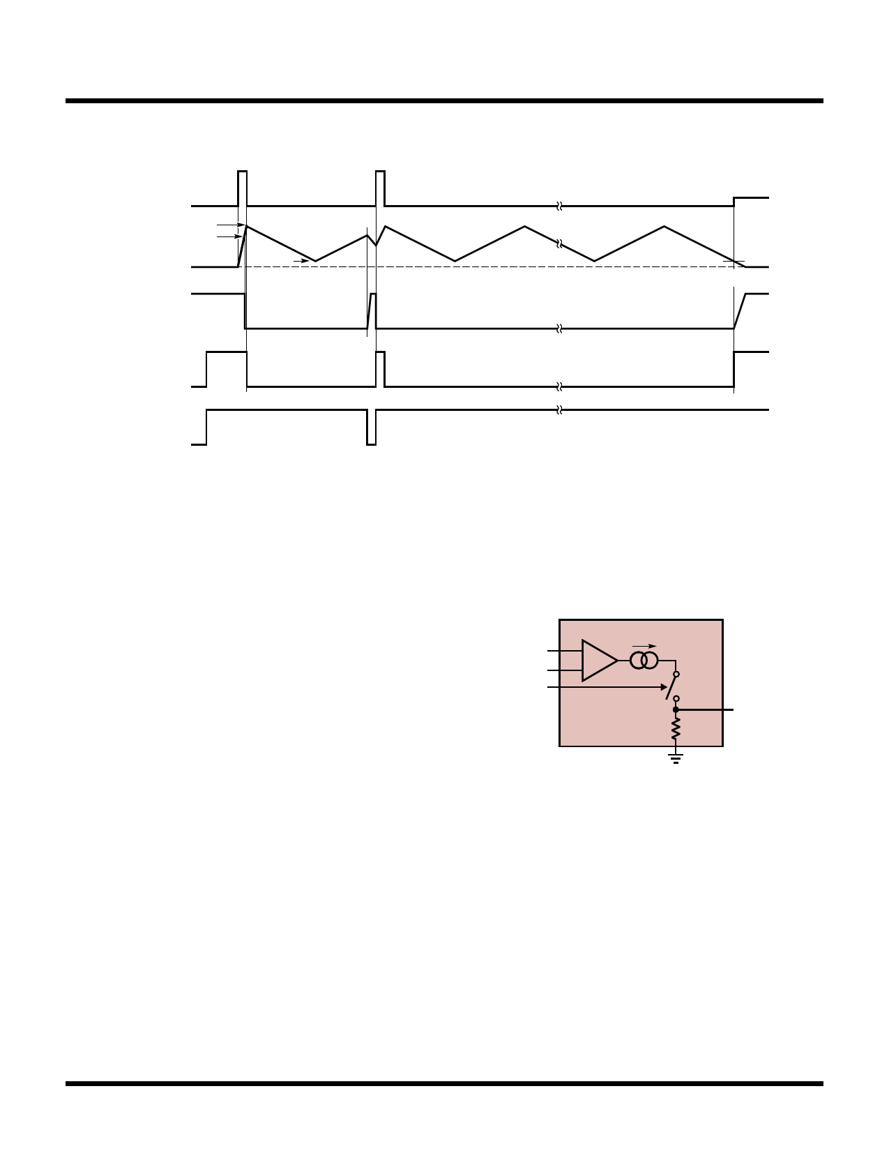
Figure 6. Auto Retry with INP Cycling Low
Fast Turn-Off Mode
If the TIMER pin is connected to VCC or any other supply
greater than 3.5V (abs max 15V), an overcurrent event
will immediately pull TGDN to TS and the LTC7000/
LTC7000-1 will remain there until the INP signal has
cycled low and then back high. In fast turn-off mode, the
typical delay from a ΔVSNS overcurrent step to TG going
low is around 70ns, so very fast short-circuit events can
be detected. Also, when the TIMER pin is connected to a
voltage greater than 3.5V, the FAULT signal is redefined to
be the inverse state of the high side pull-up (VTGUP – VTS).
The FAULT signal can be used in this application as low-
voltage digital information that has been level shifted
down from the high side MOSFET. An application for this
could include using this signal to wait until VTGUP–VTS has
gone low before turning on a redundant power MOSFET.
High Side Current Monitor Output (LTC7000 Only)
The LTC7000 contains a high side current monitor output.
The high side differential voltage sensed across the SNS+
and SNS– pins (ΔVSNS) is multiplied by 20 and ground
referenced on the IMON pin which makes it suitable for
monitoring and regulating the MOSFET current. The work-
ing range of IMON is 0V to 1.5V as ΔVSNS varies from 0mV
to 75mV. The IMON pin is a voltage output whose nominal
output impedance is 100kΩ and should not be resistively
loaded. The current monitor output is only available after
the INP signal has been high for 150µs (typical), other-
wise the IMON pin is pulled to ground. A block diagram of
the IMON circuit is shown in Figure 7. The gm of the tran-
simpedance amplifier tracks the 100kΩ internal resistor
to ground which makes variations over process minimal.
SNS+
SNS–
INP
LTC7000
+
–
gm = 200µA/V
100k
IMON
7000 F07
Figure 7. IMON Block diagram
RUN Pin and External Input Overvoltage/Undervoltage
Lockout (LTC7000 Only)
The RUN pin has two different threshold voltage levels.
Pulling RUN below 0.7V puts the LTC7000 into a low
quiescent current shutdown mode (IQ ~ 1µA). When
the RUN pin is greater than 1.21V, the part is enabled.
Figure 8 shows examples of configurations for driving
the RUN pin from logic.
The RUN and OVLO pins can alternatively be configured
as precise undervoltage (UVLO) and overvoltage (OVLO)
lockouts on the VIN supply with a resistive divider
Rev. E
16
For more information www.analog.com
Share Link: 