74LVC244A データシートの表示(PDF) - Diodes Incorporated.
部品番号
コンポーネント説明
メーカー
74LVC244A Datasheet PDF : 10 Pages
| |||
74LVC244A
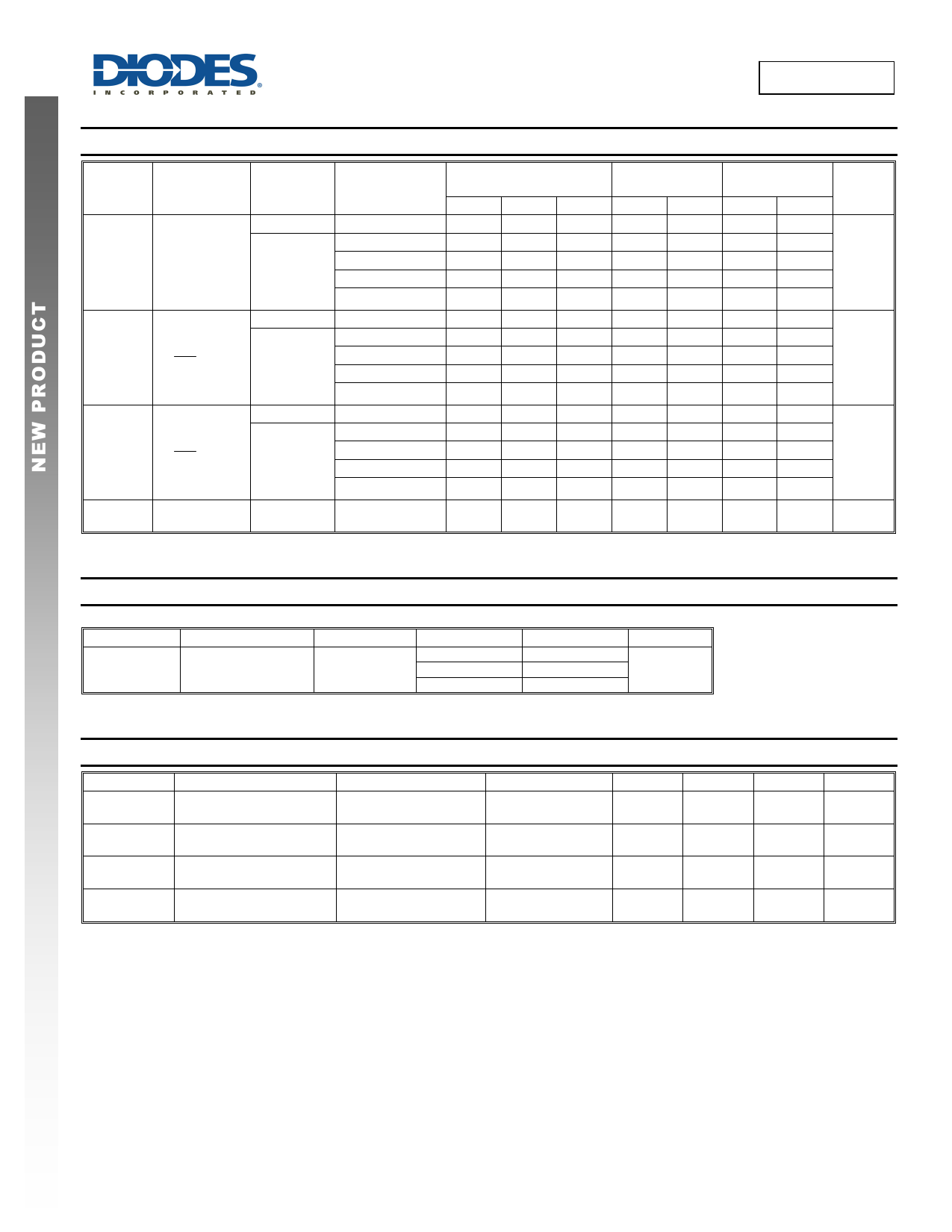
Switching Characteristics
Symbol
Parameter
Test
Conditions
VCC
TA = +25°C
TA = -40° to
+85°C
TA = -40° to
+125°C
Unit
Min
Typ
Max
Min
Max
Min
Max
1.5V
1
7
16.9
1
18.9
1
20.4
Propagation
1.8V ± 0.15V
1
6.0
11.4
1
11.3
1
12.4
tPD
Delay AN to YN Figure 1
2.5V ± 0.2V
1
3.9
7.4
1
8.0
1
10.0
ns
2.7V
1
4.2
7.7
1
8.5
1
8.8
3.3V ± 0.3
1.5
3.8
7.3
1.5
7.7
1.5
7.9
1.5V
1
12.4 18.3
1
19.8
1
25.4
1.8V ± 0.15V
1
6.4
12.1
1
12.6
1
14.1
Enable Time
tEN
OE to YN
Figure 1
2.5V ± 0.2V
2.7V
1
4.6
9.1
1
9.6
1
11.7
ns
1
5
8.4
1
8.6
1
10.3
3.3V ± 0.3
1.5
4.5
7.4
1.5
7.6
1.5
9.4
1.5V
1
7.2
15.6
1
16.1
1
17.6
1.8V ± 0.15V
1
5.8
11.6
1
12.1
1
13.6
Disable Time
tDIS
OE to YN
Figure 1
2.5V ± 0.2V
2.7V
1
3.7
7.3
1
7.8
1
9.9
ns
1
3.8
6.6
1
6.8
1
8.6
3.3V ± 0.3
1.5
3.8
6.3
1.5
6.5
1.5
8
tsk(0)
Output Skew
Time
3.3V ± 0.3
—
—
1.0
—
—
—
1.5
ns
Operating Characteristics
TA = +25°C
Symbol
Parameter
Test Conditions
VCC
Typ
Unit
Cpd
Power dissipation
F= 10 MHz
capacitance per gate Outputs Enabled
1.8V± 0.15V
2.5V± 0.2V
3.3V± 0.3V
9.9
10.2
10.6
pF
Package Characteristics
Symbol
θJA
θJC
θJA
θJC
Parameter
Thermal Resistance
Junction-to-Ambient
Thermal Resistance
Junction-to-Case
Thermal Resistance
Junction-to-Ambient
Thermal Resistance
Junction-to-Case
Package
TSSOP-20
Test Conditions
Min
Typ
Max
Unit
(Note 9)
—
74
—
°C/W
TSSOP-20
(Note 9)
—
15
—
°C/W
V-QFN4525-20
(Note 9)
—
67
—
°C/W
V-QFN4525-20
(Note 9)
—
20
—
°C/W
Note:
9. Test conditions for TSSOP-20 and V-QFN4525-20: Devices mounted on 4 layer FR-4 substrate PC board, 2oz copper, with minimum recommended
pad layout per JESD 51-7.
74LVC244A
Document number: DS35888 Rev. 1 - 2
5 of 10
www.diodes.com
July 2014
© Diodes Incorporated
Share Link: 