74LVC1G79-Q100 データシートの表示(PDF) - Nexperia B.V. All rights reserved
部品番号
コンポーネント説明
メーカー
74LVC1G79-Q100 Datasheet PDF : 15 Pages
| |||
Nexperia
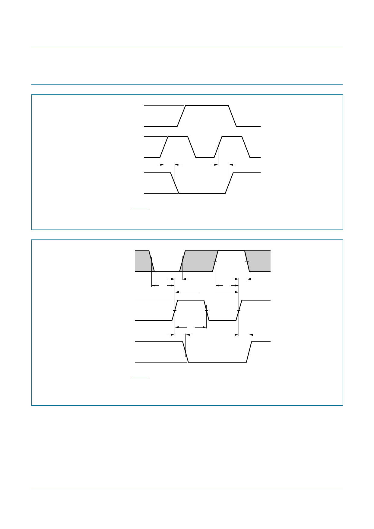
12. Waveforms
74LVC1G79-Q100
Single D-type flip-flop; positive-edge trigger
9,
'LQSXW
*1'
9,
&3LQSXW
*1'
92+
4RXWSXW
92/
90
W3+/
90
90
W3/+
90
PQD
Fig 5.
Measurement points are given in Table 9.
VOL and VOH are typical output voltage levels that occur with the output.
Clock (CP) to output (Q) propagation delay times
9,
'LQSXW
*1'
9,
&3LQSXW
*1'
92+
4RXWSXW
92/
90
WK
W VX
WK
WVX
IPD[
90
W:
W 3+/
90
W 3/+
PQD
Fig 6.
Measurement points are given in Table 9.
VOL and VOH are typical output voltage levels that occur with the output.
Clock (CP) to output (Q) propagation delay times, clock pulse width, D to set-up times, the CP to D hold
times and maximum clock pulse frequency
74LVC1G79_Q100
Product data sheet
All information provided in this document is subject to legal disclaimers.
Rev. 2 — 12 December 2016
© Nexperia B.V. 2017. All rights reserved
8 of 15
Share Link: 