74LVQ74SJX データシートの表示(PDF) - Fairchild Semiconductor
部品番号
コンポーネント説明
メーカー
74LVQ74SJX Datasheet PDF : 6 Pages
| |||
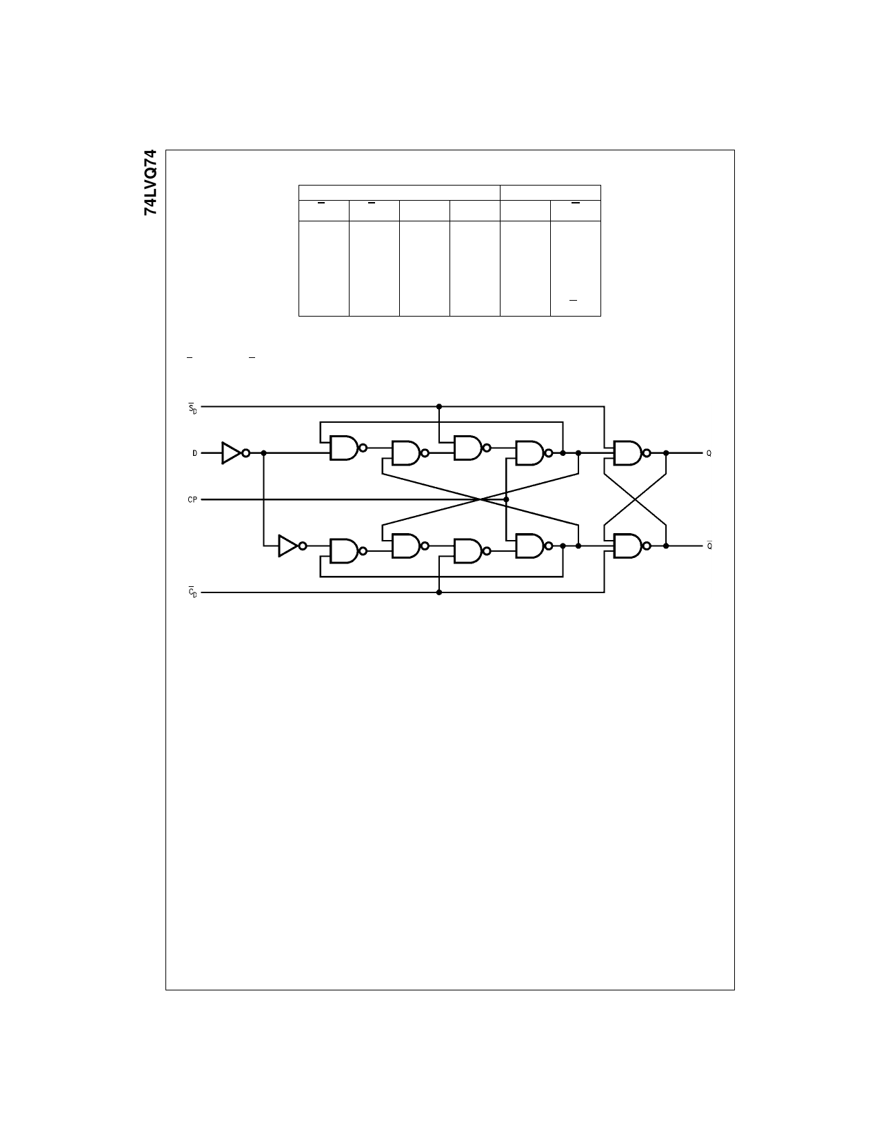
Truth Table
Inputs
Outputs
SD
CD
CP
D
Q
Q
L
H
X
X
H
L
H
L
X
X
L
H
L
H
H
L
H
H
X
X
H
L
H
H
L
H
L
H
H
H
L
H = HIGH Voltage Level
L = LOW Voltage Level
X = Immaterial
= LOW-to-HIGH Clock Transition
Q0(Q0) = Previous Q(Q) before LOW-to-HIGH Transition of Clock
X
Q0
Q0
Logic Diagram
Please note that this diagram is provided only for the understanding of logic operations and should not be used to estimate propagation delays.
www.fairchildsemi.com
2
Share Link: 