74ALVC16834ADGG データシートの表示(PDF) - NXP Semiconductors.
部品番号
コンポーネント説明
メーカー
74ALVC16834ADGG Datasheet PDF : 15 Pages
| |||
Nexperia
74ALVC16834A
18-bit registered driver with inverted register enable; 3-state
Symbol Parameter
fmax
maximum
frequency
CPD
power dissipation
capacitance
Conditions
CP; Figure 8
VCC = 2.3 V to 2.7 V
VCC = 2.7 V
VCC = 3.0 V to 3.6 V
per buffer; VI = GND to VCC
transparent mode; output enabled
transparent mode; output disabled
clocked mode; output enabled
clocked mode; output disabled
[1] Typical values are measured at Tamb = 25 °C
Typical values for VCC = 2.3 V to 2.7 V are measured at VCC = 2.5 V
Typical values for VCC = 3.0 V to 3.6 V are measured at VCC = 3.3 V
[2] tpd is the same as tPHL and tPLH.
[3] ten is the same as tPZH and tPZL.
[4] tdis is the same as tPHZ and tPLZ.
[5] CPD is used to determine the dynamic power dissipation (PD in μW):
PD = CPD × VCC2 × fi × N +∑(CL × VCC2 × fo) where:
fi = input frequency in MHz;
fo = output frequency in MHz;
CL = output load capacitance in pF;
VCC = supply voltage in V;
N = number of inputs switching;
∑(CL × VCC2 × fo) = sum of outputs.
Min
Typ [1]
Max Unit
150
300
200
350
150
300
[5]
-
13
-
3
-
22
-
15
- MHz
- MHz
- MHz
- pF
- pF
- pF
- pF
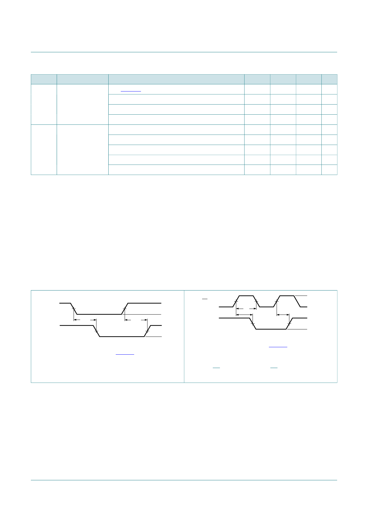
10.1 Waveforms and test circuit
An input
Yn output
VM
tPHL
VM
tPLH
VI
GND
VOH
VOL
002aac726
Measurement points are given in Table 8.
VOL and VOH are typical voltage output drop that occur with
the output load.
Figure 5. Input (An) to output (Yn) propagation delay
LE input
Yn output
VM
tw
tPHL
VM
VM
tPLH
VI
GND
VOH
VOL
002aac727
Measurement points are given in Table 8.
VOL and VOH are typical voltage output drop that occur with
the output load.
Figure 6. LE input pulse width, LE input to Yn output
propagation delays
74ALVC16834A
Product data sheet
All information provided in this document is subject to legal disclaimers.
Rev. 2 — 21 November 2017
© Nexperia B.V. 2017. All rights reserved.
8 / 15
Share Link: 