74ABT125(2010) データシートの表示(PDF) - NXP Semiconductors.
部品番号
コンポーネント説明
メーカー
74ABT125 Datasheet PDF : 15 Pages
| |||
NXP Semiconductors
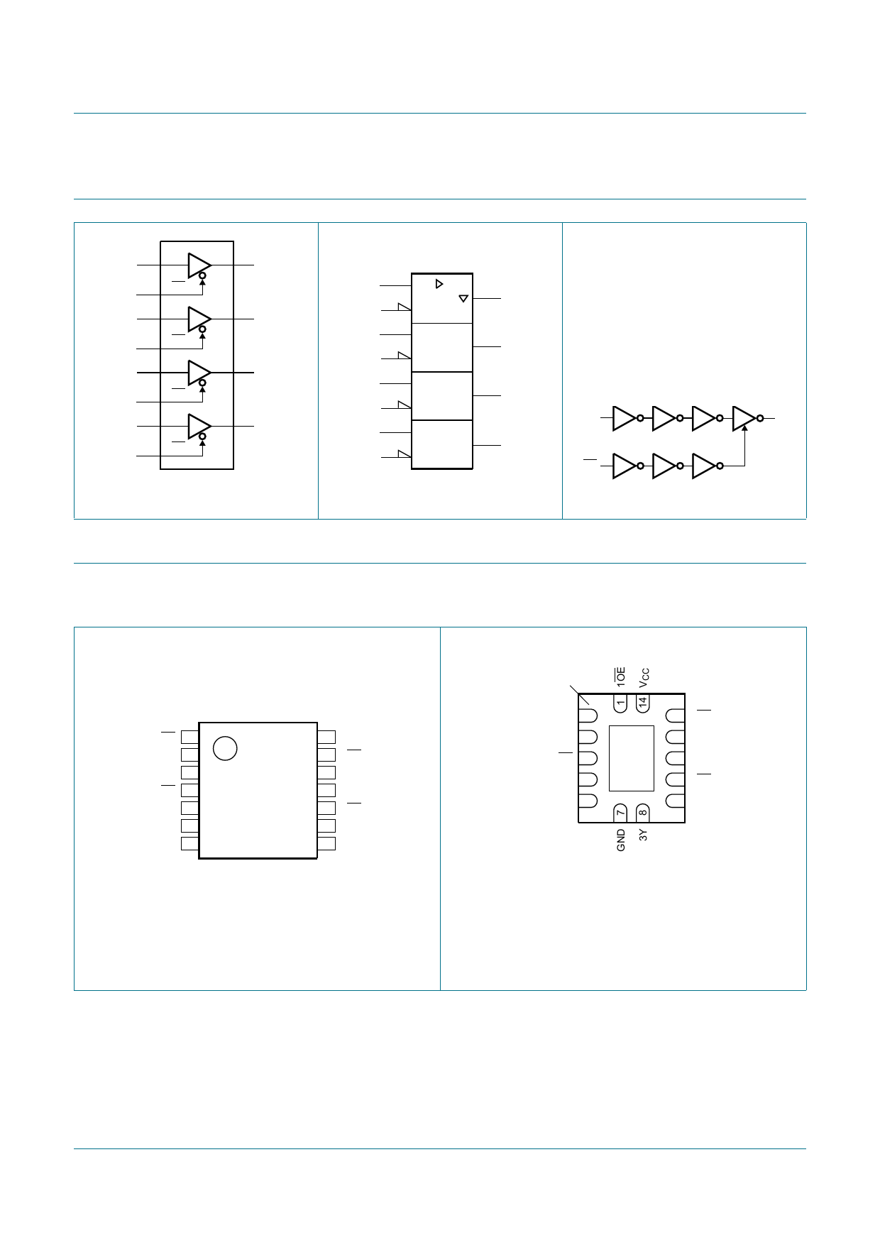
4. Functional diagram
74ABT125
Quad buffer; 3-state
2 1A
1Y 3
1 1OE
5 2A
2Y 6
4 2OE
9 3A
3Y 8
10 3OE
12 4A
4Y 11
13 4OE
mna228
Fig 1. Logic symbol
2
1
3
1
EN1
5
6
4
9
8
10
12
11
13
mna229
Fig 2. IEC logic symbol
5. Pinning information
5.1 Pinning
nA
nOE
nY
mna227
Fig 3. Logic diagram (one buffer)
1OE 1
1A 2
1Y 3
2OE 4
2A 5
2Y 6
GND 7
74ABT125
14 VCC
13 4OE
12 4A
11 4Y
10 3OE
9 3A
8 3Y
001aai027
74ABT125
terminal 1
index area
1A 2
1Y 3
2OE 4
2A 5
2Y 6
GND(1)
13 4OE
12 4A
11 4Y
10 3OE
9 3A
001aai028
Transparent top view
Fig 4. Pin configuration DIP14, SO14 and (T)SSOP14 Fig 5. Pin configuration DHVQFN14
5.2 Pin description
Table 2. Pin description
Symbol
Pin
1OE to 4OE
1, 4, 10, 13
1A to 4A
2, 5, 9, 12
1Y to 4Y
3, 6, 8, 11
GND
7
VCC
14
Description
output enable input (active LOW)
data input
data output
ground (0 V)
supply voltage
74ABT125_4
Product data sheet
All information provided in this document is subject to legal disclaimers.
Rev. 04 — 27 April 2010
© NXP B.V. 2010. All rights reserved.
2 of 15
Share Link: 