LM2903P データシートの表示(PDF) - STMicroelectronics
部品番号
コンポーネント説明
メーカー
LM2903P Datasheet PDF : 9 Pages
| |||
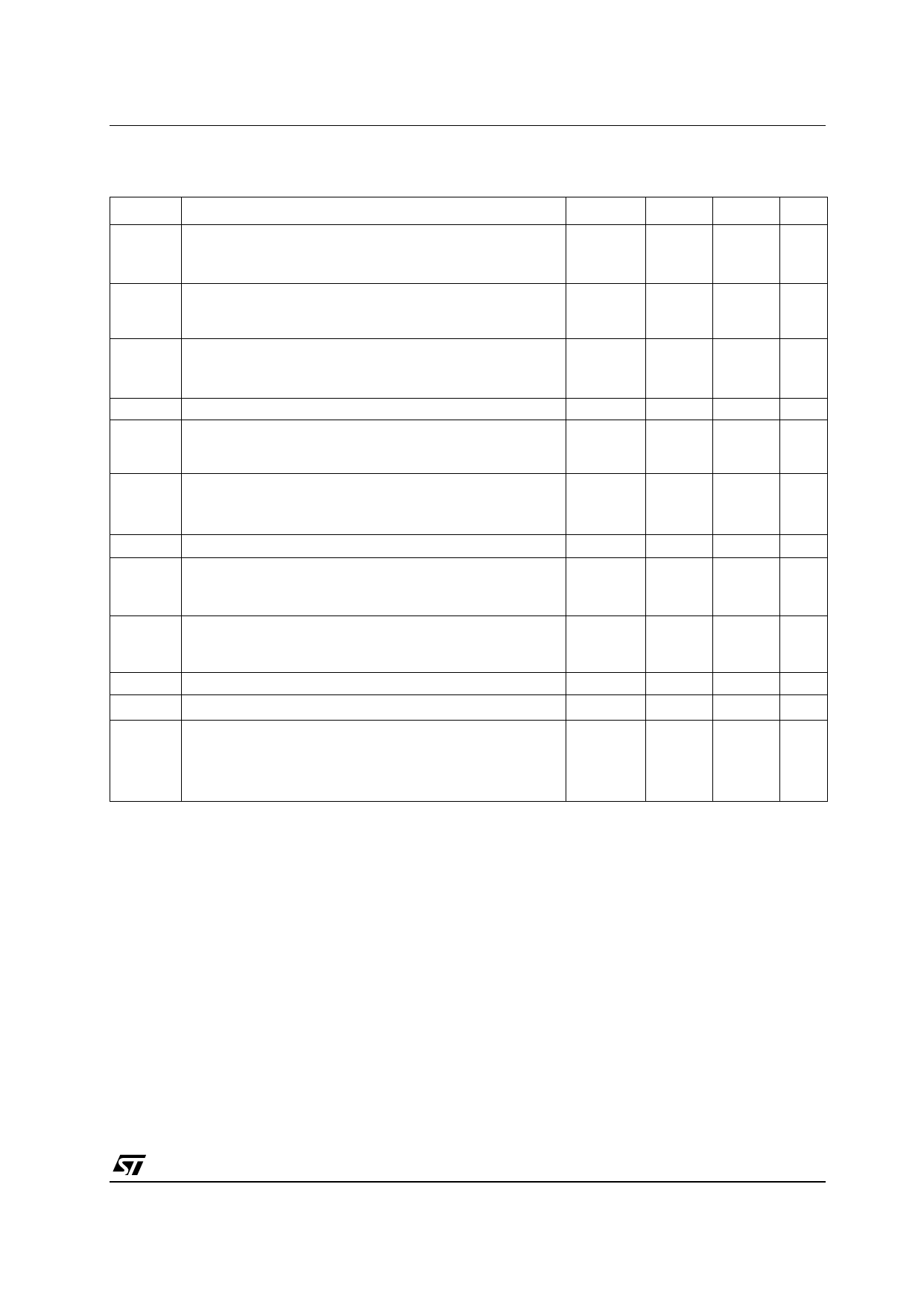
LM2903
ELECTRICAL CHARACTERISTICS
VCC+ = 5V, Vcc- = GND, Tamb = 25°C (unless otherwise specified)
Symbol
Parameter
Min.
Typ.
Max. Unit
Input Offset Voltage 1)
VIO
Tamb = +25°C
Tmin ≤ Tamb ≤ Tmax.
1
7
mV
15
Input Offset Current
IIO
Tamb = +25°C
Tmin ≤ Tamb ≤ Tmax.
5
50
nA
150
Input Bias Current 2)
IIB
Tamb = +25°C
Tmin ≤ Tamb ≤ Tmax.
25
250
nA
400
AVD Large Signal Voltage Gain (Vcc = 15V,RL=15kΩ, Vo=1 to 11V)
25
200
V/mV
ICC
VICM
Supply Current (all comparators)
VCC = 5V, no load
VCC = 30V, no load
Input Common Mode Voltage Range (Vcc= 30V) 3)
Tamb = +25°C
Tmin ≤ Tamb ≤ Tmax.
0.4
1
mA
1
2.5
0
VCC+-1.5
V
0
VCC+-2
VID Differential Input Voltage 4)
Low Level Output Voltage (Vid = -1V, Isink = 4mA)
VOL
Tamb = +25°C
Tmin ≤ Tamb ≤ Tmax
VCC+
V
250
400
mV
700
High Level Output Current (VCC =Vo =30V, Vid = 1V)
IOH
Tamb = +25°C
Tmin ≤ Tamb ≤ Tmax
0.1
nA
1
µA
ISINK Output Sink Current (Vid = -1V,Vo = 1.5V)
6
16
mΑ
tRE
Small Signal Response Time 5) (RL = 5.1kΩ to VCC+)
1.3
µs
Large Signal Response Time 6)
tREL
TTL Input (Vref = +1.4 V, RL=5.1kΩ to VCC+)
Output Signal at 50% of final value
Output Signal at 95 % of final value
500
ns
1
µs
1. At output switch point, VO ≈ 1.4V, RS = 0Ω with VCC+ from 5V to 30V, and over the full input common-mode range (0V to VCC+ –1.5V).
2. The direction of the input current is out of the IC due to the PNP input stage. This current is essentially constant, independent of the state of the
output, so no loading charge exists on the reference of input lines
3. The input common-mode voltage of either input signal voltage should not be allowed to go negative by more than 0.3V. The upper end of the
common-mode voltage range is VCC+ –1.5V, but either or both inputs can go to +30V without damage.
4. Positive excursions of input voltage may exceed the power supply level. As long as the other voltage remains within the common-mode range, the
comparator will provide a proper output state.
The low input voltage state must not be less than –0.3V (or 0.3V below the negative power supply, if used)
5. The response time specified is for a 100mV input step with 5mV overdrive.
6. Maximum values are guaranteed by design & evaluation.
3/9
Share Link: 