MT46V16M16BG-75ZL データシートの表示(PDF) - Micron Technology
部品番号
コンポーネント説明
メーカー
MT46V16M16BG-75ZL Datasheet PDF : 80 Pages
| |||
256Mb: x4, x8, x16
DDR SDRAM
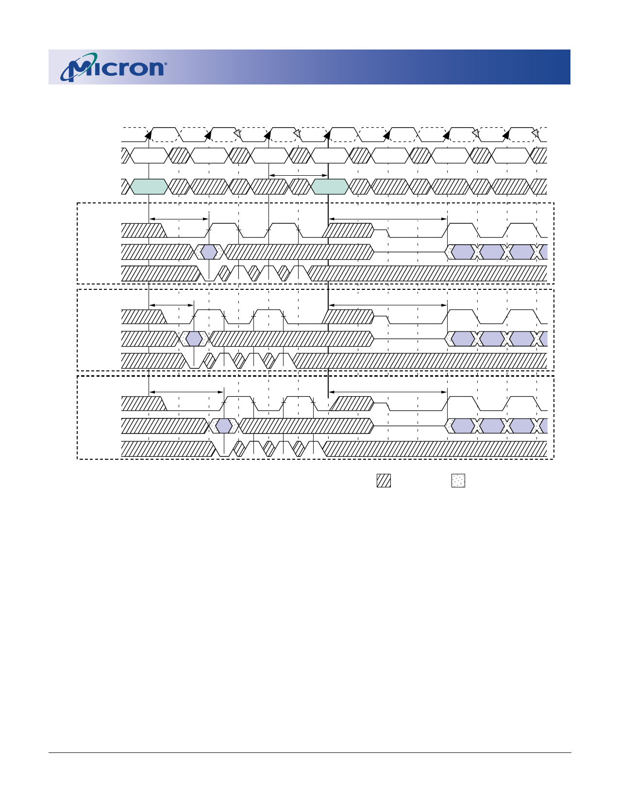
Figure 27: WRITE to READ – Odd Number of Data, Interrupting
CK#
CK
COMMAND
ADDRESS
T0
WRITE
Bank a,
Col b
T1 T1n T2 T2n T3 T3n T4
NOP
NOP
READ
NOP
tWTR
Bank a,
Col n
T5 T5n T6 T6n
NOP
NOP
tDQSS (NOM)
DQS
tDQSS
CL = 2
DQ
DI
b
DO
n
DM
tDQSS (MIN)
DQS
DQ
DM
tDQSS
DI
b
CL = 2
DO
n
tDQSS (MAX)
DQS
tDQSS
DQ
DI
b
DM
CL = 2
DO
n
DON’T CARE
TRANSITIONING DATA
NOTE:
1. DI b = data-in for column b; DO n = data-out for column n.
2. An interrupted burst of 4 is shown; one data element is written.
3. tWTR is referenced from the first positive CK edge after the last desired data-in pair (not the last two data elements).
4. A10 is LOW with the WRITE command (auto precharge is disabled).
5. DQS is required at T1n, T2, and T2n (nominal case) to register DM.
6. If the burst of 8 was used, DM and DQS would be required at T3–T3n because the READ command would not mask these
data elements.
09005aef8076894f
256MBDDRx4x8x16_2.fm - Rev. F 6/03 EN
36
Micron Technology, Inc., reserves the right to change products or specifications without notice.
©2003 Micron Technology, Inc.
Share Link: 