4926N データシートの表示(PDF) - ON Semiconductor
部品番号
コンポーネント説明
メーカー
4926N Datasheet PDF : 7 Pages
| |||
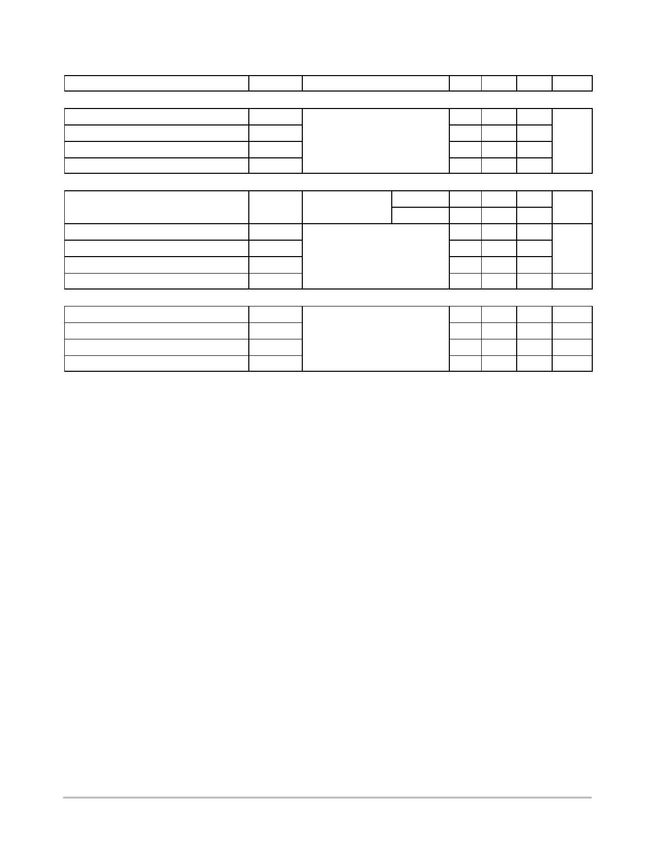
NTMFS4926N
ELECTRICAL CHARACTERISTICS (TJ = 25°C unless otherwise specified)
Parameter
Symbol
Test Condition
Min Typ Max Unit
SWITCHING CHARACTERISTICS (Note 6)
Turn−On Delay Time
td(ON)
Rise Time
tr
Turn−Off Delay Time
td(OFF)
Fall Time
tf
DRAIN−SOURCE DIODE CHARACTERISTICS
VGS = 10 V, VDS = 15 V,
ID = 15 A, RG = 3.0 W
6.6
31.8
ns
18.3
4.0
Forward Diode Voltage
Reverse Recovery Time
Charge Time
Discharge Time
Reverse Recovery Charge
PACKAGE PARASITIC VALUES
VSD
tRR
ta
tb
QRR
VGS = 0 V,
IS = 30 A
TJ = 25°C
TJ = 125°C
VGS = 0 V, dIS/dt = 100 A/ms,
IS = 30 A
0.87 1.1
V
0.76
21.9
11.0
ns
10.9
8.0
nC
Source Inductance
LS
Drain Inductance
Gate Inductance
LD
LG
TA = 25°C
Gate Resistance
RG
5. Pulse Test: pulse width v 300 ms, duty cycle v 2%.
6. Switching characteristics are independent of operating junction temperatures.
1.00
nH
0.005
nH
1.84
nH
1.0
2.2
W
http://onsemi.com
3
Share Link: 