M74HC4538RM13TR データシートの表示(PDF) - STMicroelectronics
部品番号
コンポーネント説明
メーカー
M74HC4538RM13TR Datasheet PDF : 18 Pages
| |||
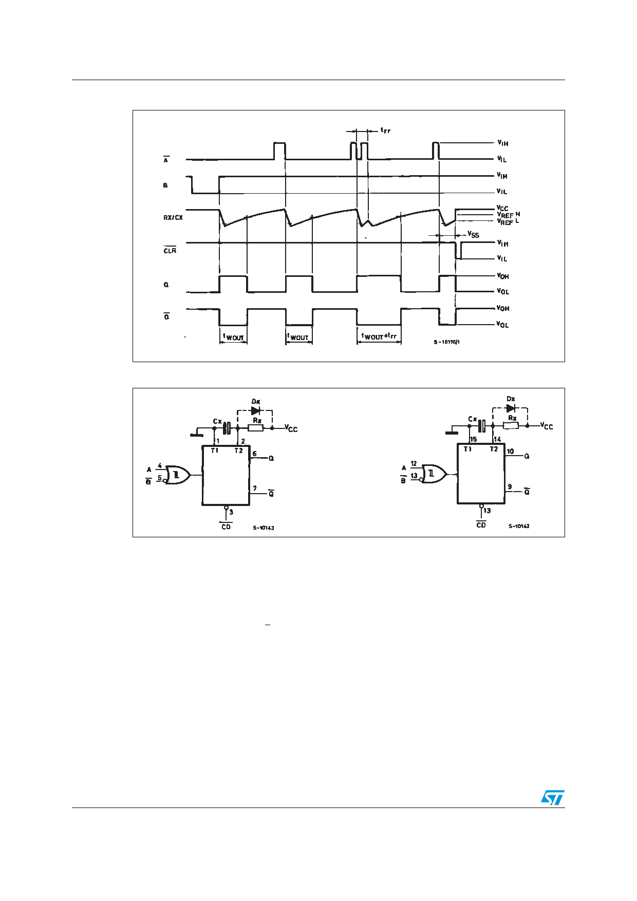
Pin connection and IEC logic symbols
Figure 4. Timing chart
M74HC4538
Figure 5. Block diagram
1. Cx, Rx, Dx are external components.
2. Dx is a clamping diode.
The external capacitor is charged to VCC in the standby state, i.e. no trigger. When the supply voltage is
turned off Cx is discharged mainly through an internal parasitic diode (see figures). If Cx is sufficiently large
and VCC decreases rapidly, there will be some possibility of damaging the IC with a surge current or latch-
up. If the voltage supply filter capacitor is large enough and VCC decreases slowly, the surge current is
automatically limited and damage to the IC is avoided. The maximum forward current of the parasitic diode
is approximately 20 mA. In cases where Cx is large the time taken for the supply voltage to fall to 0.4 VCC
can be calculated as follows: tf > (VCC - 0.7) x Cx/20 mA.
In cases where tf is too short an external clamping diode is required to protect the IC from the surge
current.
4/18
Share Link: 