NTMFS4935N データシートの表示(PDF) - ON Semiconductor
部品番号
コンポーネント説明
メーカー
NTMFS4935N Datasheet PDF : 9 Pages
| |||
NTMFS4935N
MOSFET – Power, Single,
N-Channel, SO-8 FL
30 V, 93 A
Features
• Low RDS(on) to Minimize Conduction Losses
• Low Capacitance to Minimize Driver Losses
• Optimized Gate Charge to Minimize Switching Losses
• These Devices are Pb−Free, Halogen Free/BFR Free and are RoHS
Compliant
Applications
• CPU Power Delivery, DC−DC Converters
MAXIMUM RATINGS (TJ = 25°C unless otherwise stated)
Parameter
Symbol Value Unit
Drain−to−Source Voltage
Gate−to−Source Voltage
Continuous Drain
Current RqJA
(Note 1)
VDSS
30
V
VGS
±20
V
TA = 25°C
ID
21.8
A
TA = 100°C
13.8
Power Dissipation
RqJA (Note 1)
TA = 25°C
PD
2.63
W
Continuous Drain
Current RqJA ≤
10 s (Note 1)
TA = 25°C
ID
TA = 100°C
40
A
25
Power Dissipation
TA = 25°C
PD
RqJA ≤ 10 s
(Note 1)
Steady
State
Continuous Drain
TA = 25°C
ID
Current RqJA
(Note 2)
TA = 100°C
8.7
W
13
A
8.2
Power Dissipation
RqJA (Note 2)
Continuous Drain
Current RqJC
(Note 1)
TA = 25°C
PD
TC = 25°C
ID
TC = 85°C
0.93
W
93
A
59
Power Dissipation
RqJC (Note 1)
TC = 25°C
PD
48
W
Pulsed Drain
Current
TA = 25°C, tp = 10 ms
IDM
275
A
Current Limited by Package
TA = 25°C
Operating Junction and Storage
Temperature
IDmax
TJ,
TSTG
100
A
−55 to °C
+150
Source Current (Body Diode)
Drain to Source DV/DT
IS
dV/dt
44
A
6
V/ns
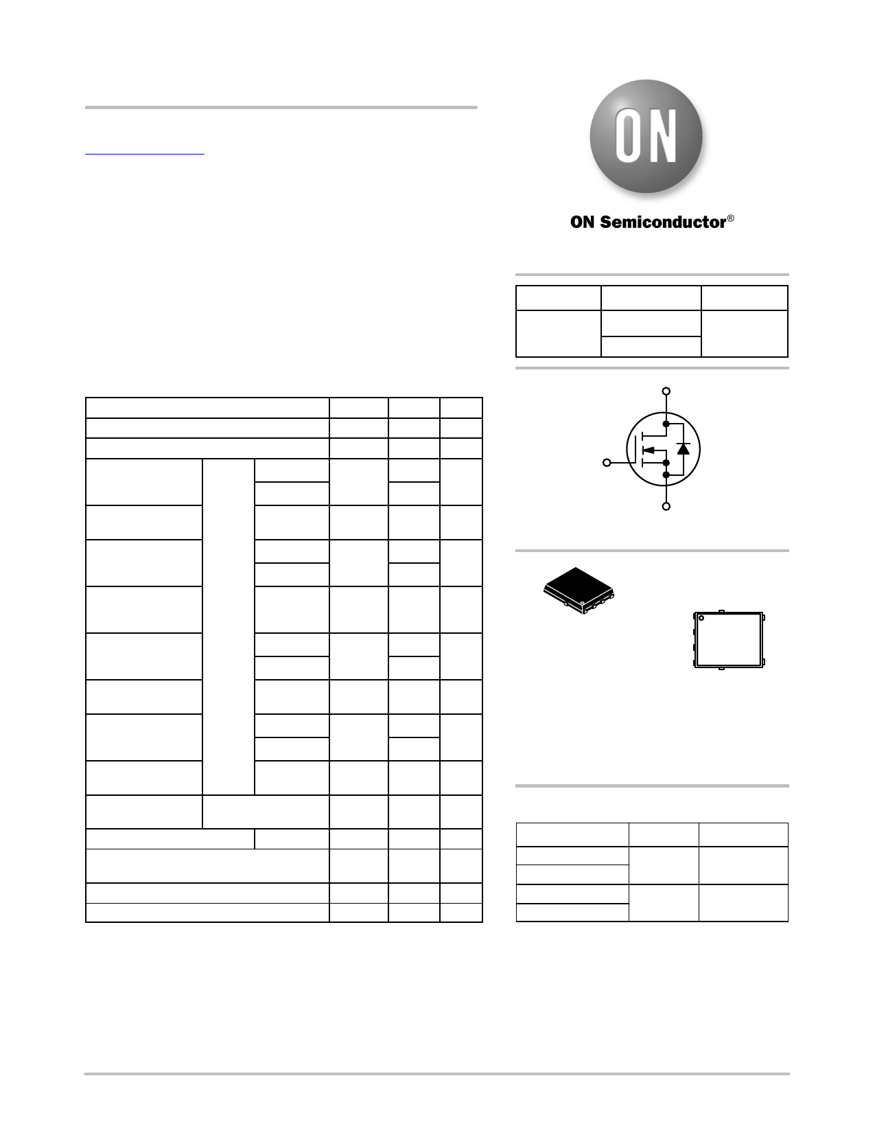
http://onsemi.com
V(BR)DSS
30 V
RDS(ON) MAX
3.2 mW @ 10 V
4.2 mW @ 4.5 V
ID MAX
93 A
D (5,6)
G (4)
S (1,2,3)
N−CHANNEL MOSFET
1
SO−8 FLAT LEAD
CASE 488AA
STYLE 1
MARKING
DIAGRAM
D
S
D
S 4935N
S AYWZZ
G
D
D
A
= Assembly Location
Y
= Year
W
= Work Week
ZZ
= Lot Traceability
ORDERING INFORMATION
Device
Package
Shipping†
NTMFS4935NT1G SO−8 FL
NTMFS4935NCT1G (Pb−Free)
1500 /
Tape & Reel
NTMFS4935NT3G SO−8 FL
NTMFS4935NCT3G (Pb−Free)
5000 /
Tape & Reel
†For information on tape and reel specifications,
including part orientation and tape sizes, please
refer to our Tape and Reel Packaging Specifications
Brochure, BRD8011/D.
© Semiconductor Components Industries, LLC, 2012
1
May, 2019 − Rev. 10
Publication Order Number:
NTMFS4935N/D
Share Link: 