TC7MPN3245FTG(2007) データシートの表示(PDF) - Toshiba
部品番号
コンポーネント説明
メーカー
TC7MPN3245FTG Datasheet PDF : 22 Pages
| |||
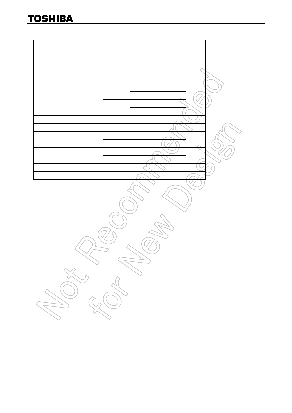
Absolute Maximum Rating (Note 1)
TC7MPN3245FTG
Characteristics
Symbol
Rating
Unit
Power supply voltage
(Note 2)
DC input voltage
(DIR, OE )
DC bus I/O voltage
Input diode current
Output diode current
DC output current
DC VCC/ground current per supply pin
Power dissipation
Storage temperature
VCCA
VCCB
VIN
VI/OA
VI/OB
IIK
II/OK
IOUTA
IOUTB
ICCA
ICCB
PD
Tstg
−0.5 to 4.6
V
−0.5 to 4.6
−0.5 to 4.6
V
−0.5 to 4.6 (Note 3)
−0.5 to VCCA + 0.5 (Note 4)
V
−0.5 to 4.6 (Note 3)
−0.5 to VCCB + 0.5 (Note 4)
−50
mA
±50 (Note 5) mA
±25
mA
±6
±50
mA
±50
180
mW
−65 to 150
°C
Note 1:
Exceeding any of the absolute maximum ratings, even briefly, may lead to deterioration in IC performance
or even destruction.
Using continuously under heavy loads (e.g. the application of high temperature/current/voltage and the
significant change in temperature, etc.) may cause this product to decrease in the reliability significantly
even if the operating conditions (i.e. operating temperature/current/voltage, etc.) are within the absolute
maximum ratings and the operating ranges.
Please design the appropriate reliability upon reviewing the Toshiba Semiconductor Reliability Handbook
(“Handling Precautions”/“Derating Concept and Methods”) and individual reliability data (i.e. reliability test
report and estimated failure rate, etc).
Note 2: Do not supply a voltage to VCCB pin when VCCA is in the OFF state.
Note 3: Output in OFF state
Note 4: High or Low state. IOUT absolute maximum rating must be observed.
Note 5: VOUT < GND, VOUT > VCC
4
2007-10-19
Share Link: 