NCV551SN14T1G(2013) データシートの表示(PDF) - ON Semiconductor
部品番号
コンポーネント説明
メーカー
NCV551SN14T1G Datasheet PDF : 11 Pages
| |||
NCP551, NCV551
Input
Q1
R
1
1.0 mF
2
3
Output Input
Q2
R1
Q1
R2
R3
5
1
1.0 mF
1.0 mF
2
4
3
Output
5
1.0 mF
4
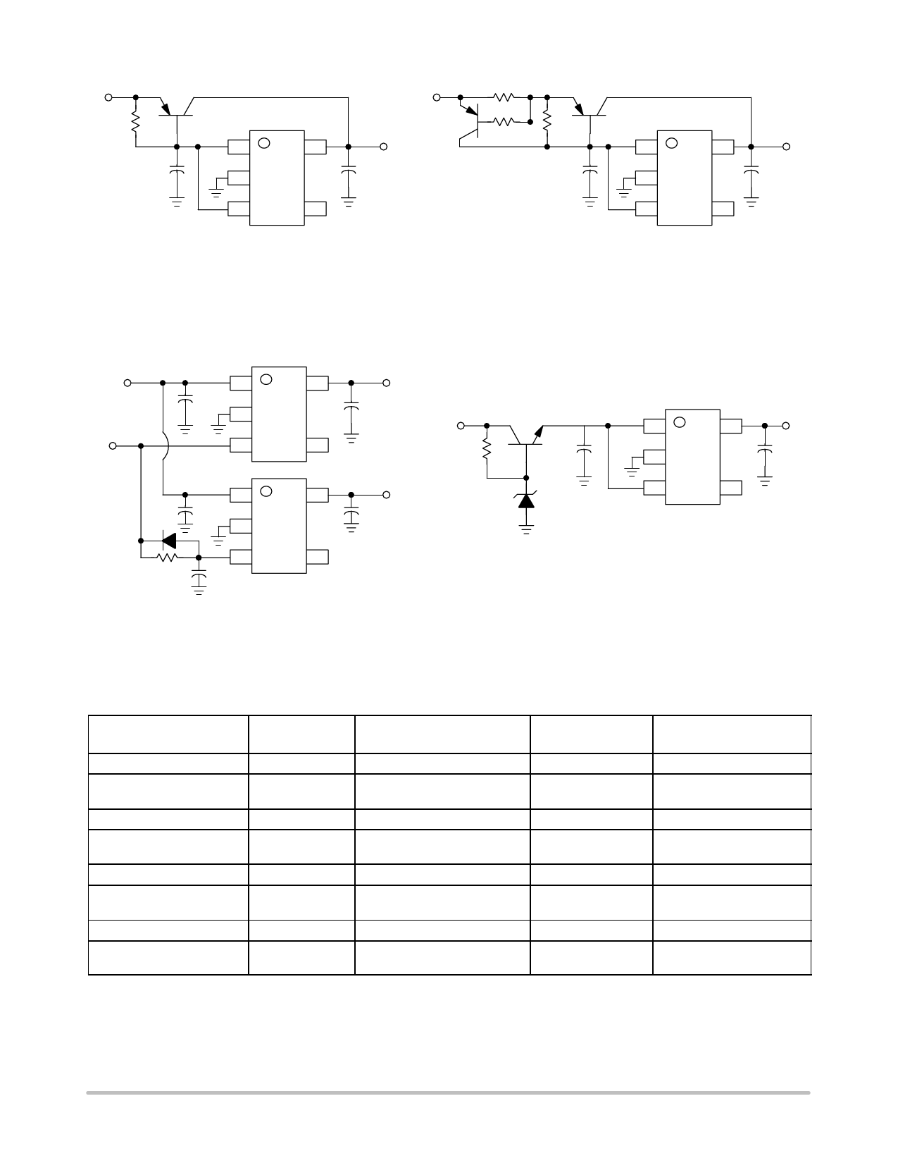
Figure 21. Current Boost Regulator
The NCP551 series can be current boosted with a PNP transist-
or. Resistor R in conjunction with VBE of the PNP determines
when the pass transistor begins conducting; this circuit is not
short circuit proof. Input/Output differential voltage minimum is
increased by VBE of the pass resistor.
Input
Enable
1
1.0 mF
2
3
Output
5
1.0 mF
4
1
1.0 mF
2
3
R
C
Output
5
1.0 mF
4
Figure 23. Delayed Turn−on
If a delayed turn−on is needed during power up of several
voltages then the above schematic can be used. Resistor R,
and capacitor C, will delay the turn−on of the bottom regulator.
Figure 22. Current Boost Regulator with
Short Circuit Limit
Short circuit current limit is essentially set by the VBE of Q2 and
R1. ISC = ((VBEQ2 − ib * R2) / R1) + IO(max) Regulator
Input
R
Q1
1.0 mF
11 V
Output
1
5
1.0 mF
2
3
4
Figure 24. Input Voltages Greater than 12 V
A regulated output can be achieved with input voltages that
exceed the 12 V maximum rating of the NCP551 series with
the addition of a simple pre−regulator circuit. Care must be
taken to prevent Q1 from overheating when the regulated
output (Vout) is shorted to GND.
http://onsemi.com
9
Share Link: 