74VHC161284CM データシートの表示(PDF) - Fairchild Semiconductor
部品番号
コンポーネント説明
メーカー
74VHC161284CM Datasheet PDF : 11 Pages
| |||
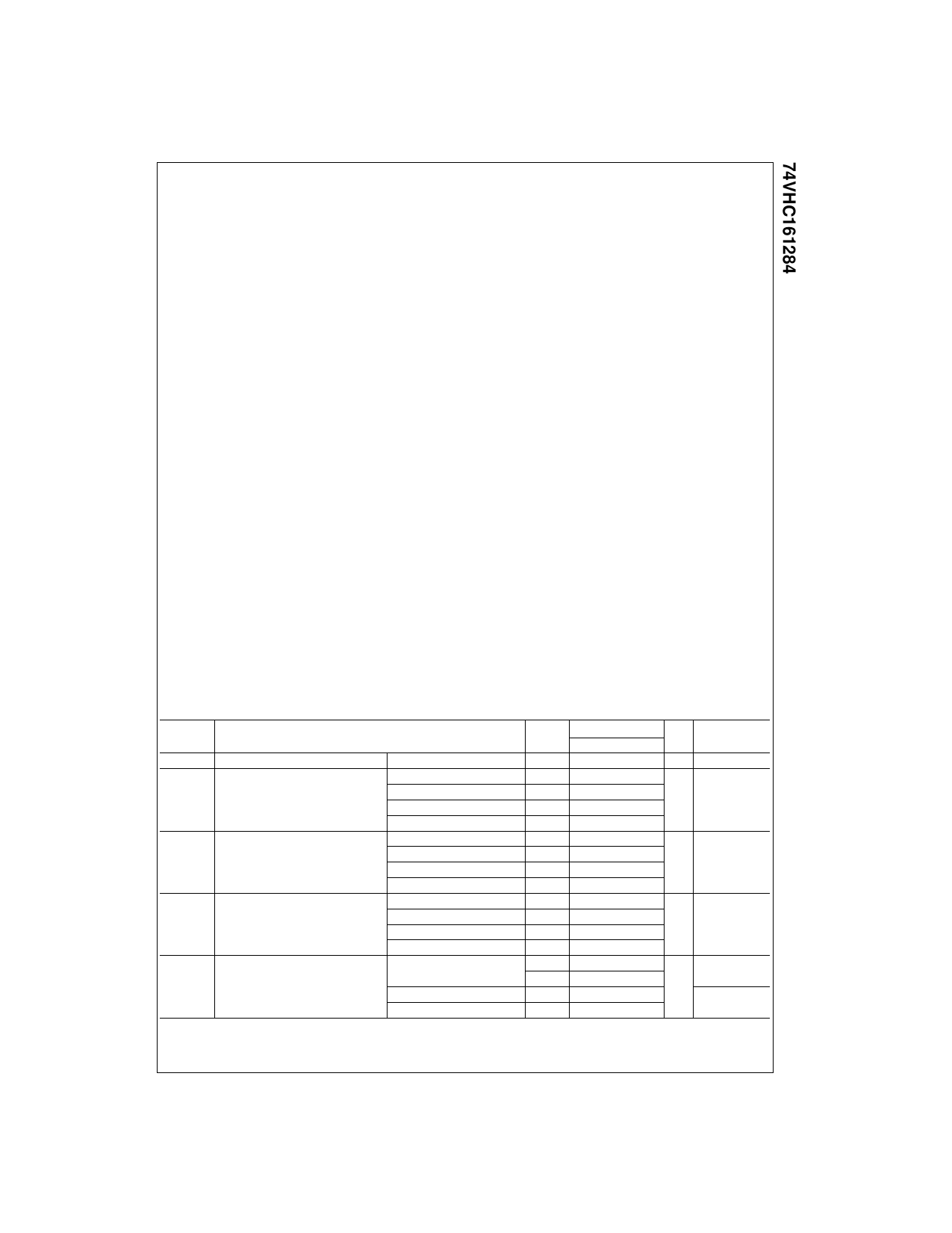
Absolute Maximum Ratings(Note 3)
Supply Voltage
VCC
Input Voltage (VI) (Note 4)
A1–A 13, PLHIN, DIR, HD
B1–B8, C14–C17, HLHIN
B1–B8, C14–C17, HLHIN
Output Voltage (VO)
A1–A8, A14–A17, HLH
B1–B 8, Y9–Y13, PLH
B1–B 8, Y9–Y13, PLH
DC Output Current (IO)
A1–A8, HLH
B1–B8, Y9–Y13
PLH (Output LOW)
PLH (Output HIGH)
Input Diode Current (IIK) (Note 4)
DIR, HD, A9–A13,
PLH, HLH, C14–C17
Output Diode Current (IOK)
A1–A8, A14–A17, HLH
B1–B8, Y9–Y13, PLH
DC Continuous VCC or
Ground Current
Storage Temperature
ESD (HBM) Last Passing
Voltage
−0.5V to + 7.0V
−0.5V to VCC + 0.5V
−0.5V to + 5.5V (DC)
−2.0V to + 7.0V *
*40 ns Transient
−0.5V to VCC + 0.5V
−0.5V to + 5.5V (DC)
−2.0V to + 7.0V*
*40 ns Transient
±25 mA
±50 mA
84 mA
−50 mA
−20 mA
±50 mA
−50 mA
±200 mA
−65°C to + 150°C
2000V
Recommended Operating
Conditions
Supply Voltage
VCC
DC Input Voltage (VI)
Open Drain Voltage (VO)
Operating Temperature (TA)
4.5V to 5.5V
0V to VCC
0V to 5.5V
−40°C to + 85°C
Note 3: Absolute Maximum continuos ratings are those values beyond
which damage to the device may occur. Exposure to these indicated may
adversely affect device reliability. Functional operation under absolute max-
imum rated conditions is not implied.
Note 4: Either voltage limit or current limit is sufficient to protect inputs.
DC Electrical Characteristics
Symbol
Parameter
VIK
Input Clamp Diode Voltage
VIH
Minimum HIGH Level Input Voltage
An, PLHIN, DIR, HD
Bn
Cn
HLHIN
VIL
Maximum LOW Level Input Voltage
An, PLHIN, DIR, HD
Bn
Cn
HLHIN
∆VT
Minimum Input Hysteresis
An, PLHIN, DIR, HD
Bn
Cn
HLHIN
VOH
Minimum HIGH Level Output Voltage An, HLH
Bn, Yn
PLH
VCC TA = −40°C to +85°C Units Conditions
(V) Guaranteed Limits
3.0
4.5 − 5.5
4.5 − 5.5
4.5 − 5.5
−1.2
0.7 VCC
2.0
2.3
V II = −18 mA
V
4.5 − 5.5
2.6
4.5 − 5.5
0.3 VCC
4.5 − 5.5
0.8
V
4.5 − 5.5
0.8
4.5 − 5.5
1.6
4.5 − 5.5
0.4
4.5 − 5.5
0.4
5.0
0.8
5.0
0.3
4.5
4.4
4.5
3.8
4.5
3.73
4.5
4.45
VT + –VT−
V VT+ –VT−
VT + –VT−
VT + –VT−
IOH = −50 µA
V IOH = −8 mA
IOH = −14 mA
IOH = −500 µA
3
www.fairchildsemi.com
Share Link: 