BM29F400B データシートの表示(PDF) - Unspecified
部品番号
コンポーネント説明
メーカー
BM29F400B Datasheet PDF : 38 Pages
| |||
BRIGHT
Microelectronics
Inc.
Preliminary BM29F400T/BM29F400B
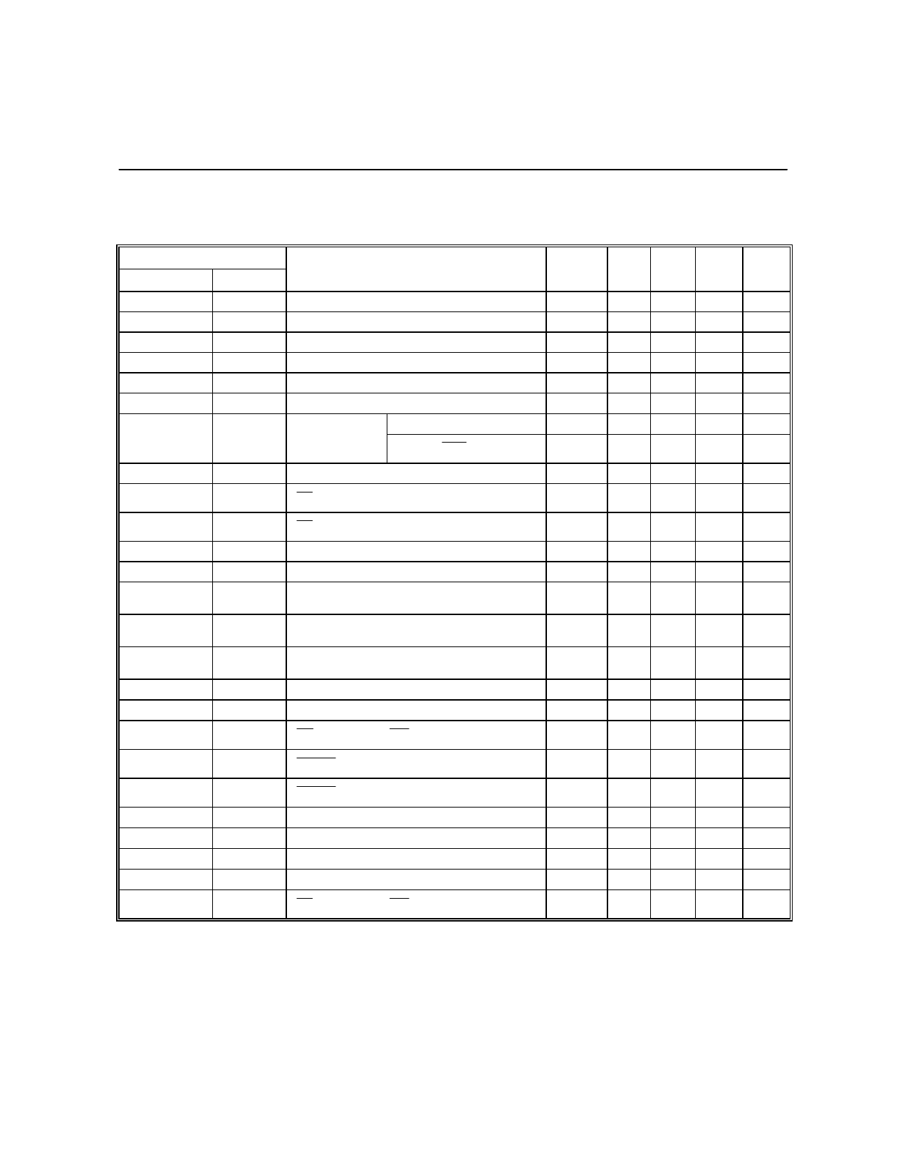
AC CHARACTERISTICS
Programming/Erase Operations
PARAMETER SYM.
DESCRIPTION
JEDEC
tAVAV
tAVWL
tWLAX
tDVWH
tWHDX
Standard
tWC
tAS
tAH
tDS
tDH
tOES
tOEH
Write Cycle Time(1)
Address Setup Time
Address Hold Time
Data Setup Time
Data Hold Time
Output Enable Setup Time
Output Enable
Read(1)
Hold Time
Toggle & Data Polling(1)
tGHWL
tELWL
tGHWL
tCS
Read Recover Time Before Write
CE Setup Time
tWHEH
tCH
CE Hold Time
tWLWH
tWHWL
tWHWH1
tWP
tWPH
tWHWH1
Write Pulse Width
Write Pulse Width High
Byte Programming Operation
tWHWH2
tWHWH2 Sector Erase Operation(2)
tWHWH3
tWHWH3 Chip Erase Operation(2)
tVCS
tVIDR
tOESP
Vcc Setup Time(1)
Rise Time to VID(1,3)
OE Setup Time to WE Active(1, 3, 4)
tRP
RESET Pulse Width
tRSP
tBUSY
tVLHT
tWPP1
tWPP2
tCSP
RESET Setup Time( 3)
Programming/Erase Valid to RY/BY Delay(1)
Voltage Transition Time(1, 4)
Sector Protect Write Pulse Width(4)
Sector Unprotect Write Pulse Width(4)
CE Setup Time to WE Active(1, 4)
Notes:
1. Not 100% tested.
2. Does not include pre-programming time.
3. This timing is for Temporary Sector Unprotect operation.
These timings are for Sector Protect and/or Sector Unprotect operations.
-90 -120 -150 UNIT
Min.
90
120
150
nS
Min.
0
0
0
nS
Min.
45
50
50
nS
Min.
45
50
50
nS
Min.
0
0
0
nS
Min.
0
0
0
nS
Min.
0
0
0
nS
Min.
10
10
10
nS
Min.
0
0
0
nS
Min.
0
0
0
nS
Min.
0
0
0
nS
Min.
45
50
50
nS
Min.
20
20
20
nS
Typ.
16
16
16
uS
Max.
400 400
400
uS
Typ. Max. 0.26 0.26 0.26
sec
12
12
12
Typ.
2.0
2.0
2.0
sec
Max.
90
90
90
Min.
50
50
50
mS
Min.
500 500
500
nS
Min.
4
4
4
mS
Min.
500 500
500
nS
Min.
4
4
4
uS
Min.
40
50
60
nS
Min.
4
4
4
mS
Min.
100 100
100
mS
Min.
350 350
350
mS
Min.
4
4
4
nS
A Winbond Company
- 25 -
Publication Release Date: May 1999
Revision A1
Share Link: 