PCF8563 データシートの表示(PDF) - Tiger Electronic
部品番号
コンポーネント説明
メーカー
PCF8563 Datasheet PDF : 23 Pages
| |||
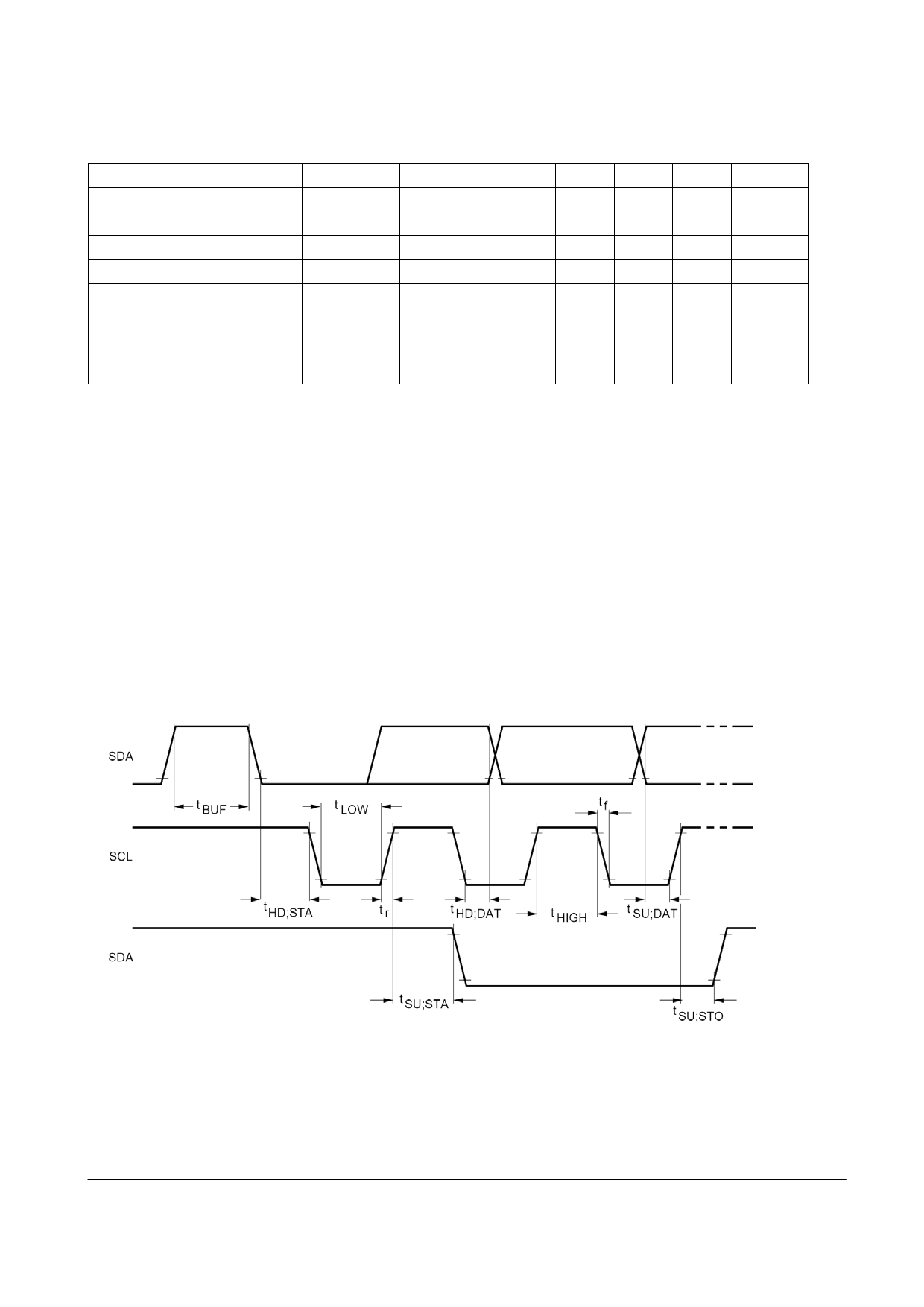
PCF8563
Characteristics
SCL and SDA rise time
SCL and SDA fall time
Capacitive bus line load
Data set-up time
Data hold time
Set-up time for STOP
condition
Tolerable spike width
on bus
Symbol
tr
tf
Cb
t S U ; D AT
t H D ; D AT
t SU;STO
t SW
Test conditions
Min Typ. Max
0.3
0.3
400
100
0
4.0
50
Unit
µs
µs
pF
ns
ns
µs
µs
*1 Unspecified for f CLKOUT = 32.768 kHz.
*2 All timing values are valid within the operating supply voltage range at Tamb and
referenced to V IL and V IH with an input voltage swing of V SS to V DD .
*3 I 2 C-bus access time between two STARTs or between a START and a STOP condition
to this device must be less than one second.
I2C-bus timing waveforms
6/23
Share Link: 