MC100EP01 データシートの表示(PDF) - ON Semiconductor
部品番号
コンポーネント説明
メーカー
MC100EP01 Datasheet PDF : 10 Pages
| |||
MC10EP01, MC100EP01
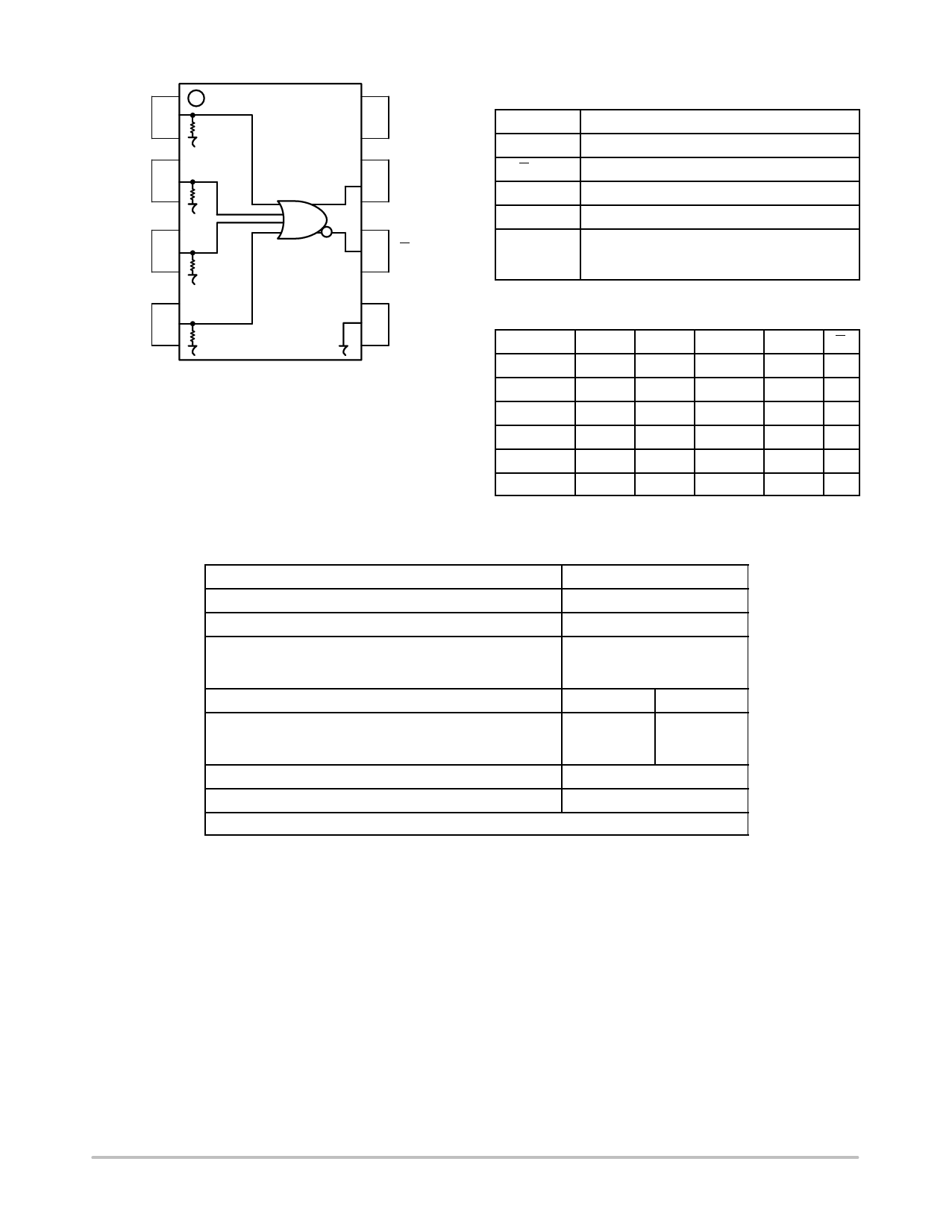
D0 1
D1 2
D2 3
8 VCC
7Q
6Q
Table 1. PIN DESCRIPTION
Pin
Function
D0 − D3
ECL Data Inputs
Q, Q
ECL Data Outputs
VCC
Positive Supply
VEE
Negative Supply
EP
Exposed pad must be connected to a sufficient
thermal conduit. Electrically connect to the most
negative supply or leave floating open.
D3 4
5 VEE
Figure 1. 8−Lead Pinout (Top View)
and Logic Diagram
Table 2. TRUTH TABLE
D0*
D1*
D2*
D3*
L
L
L
L
H
X
X
X
X
H
X
X
X
X
H
X
X
X
X
H
H
H
H
H
*Pins will default LOW when left open.
Table 3. ATTRIBUTES
Characteristics
Internal Input Pulldown Resistor
Internal Input Pullup Resistor
ESD Protection
Human Body Model
Machine Model
Charged Device Model
Moisture Sensitivity, Indefinite Time Out of Drypack (Note 1)
SOIC−8
TSSOP−8
DFN8
Flammability Rating
Oxygen Index: 28 to 34
Transistor Count
Meets or exceeds JEDEC Spec EIA/JESD78 IC Latchup Test
1. For additional information, see Application Note AND8003/D.
Value
75 kW
N/A
> 4 kV
> 200 V
> 2 kV
Pb Pkg
Pb−Free Pkg
Level 1
Level 1
Level 1
Level 1
Level 3
Level 1
UL 94 V−0 @ 0.125 in
115 Devices
Q
Q
L
H
H
L
H
L
H
L
H
L
H
L
http://onsemi.com
2
Share Link: 