IL66B(2004) データシートの表示(PDF) - Vishay Semiconductors
部品番号
コンポーネント説明
メーカー
IL66B Datasheet PDF : 5 Pages
| |||
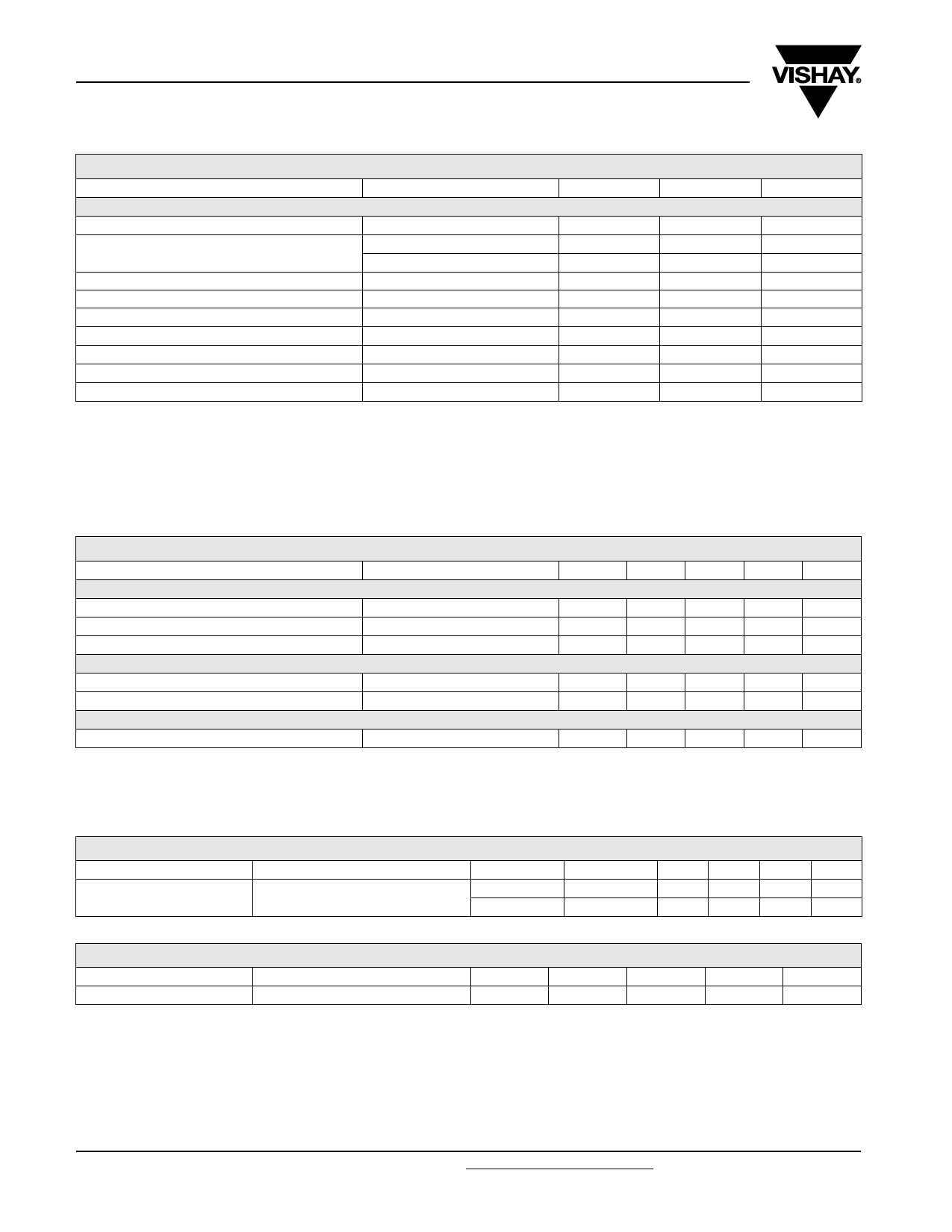
IL66B
Vishay Semiconductors
Output
Parameter
Collector-emitter breakdown voltage
Emitter-collector breakdown voltage
Power dissipation
Derate linearly from 25 °C
Test condition
Coupler
Parameter
Isolation test voltage
Isolation resistance
Total dissipation
Derate linearly
Creepage path
Clearance path
Storage temperature
Operating temperature
Lead soldering time
Test condition
t = 1.0 sec.
VIO = 500 V, Tamb = 25 °C
VIO = 500 V, Tamb = 100 °C
from 25 °C
at 260 °C
Symbol
BVCEO
BVECO
Pdiss
Symbol
VISO
RIO
RIO
Ptot
Tstg
Tamb
Tsld
Value
60
5.0
200
2.6
Value
5300
≥ 1012
≥ 1011
250
3.3
7
7
- 55 to + 150
- 55 to + 100
10
Unit
V
V
mW
mW/°C
Unit
VRMS
Ω
Ω
mW
mW/°C
min mm
min mm
°C
°C
sec.
Electrical Characteristics
Tamb = 25 °C, unless otherwise specified
Minimum and maximum values are testing requirements. Typical values are characteristics of the device and are the result of engineering
evaluation. Typical values are for information only and are not part of the testing requirements.
Input
Parameter
Forward voltage
Reverse current
Capacitance
Test condition
IF = 10 mA
VR = 3.0 V
VR = 0
Symbol
Min
Typ.
Max
Unit
VF
1.25
1.5
V
IR
0.01
100
µA
CO
25
pF
Output
Parameter
Collector-emitter breakdown
voltage
Collector-emitter leakage
current
Test condition
IC = 100 µA
VCE = 50 V, IF = 0
Symbol
Min
Typ.
Max
Unit
BVCEO
60
V
ICEO
1.0
100
nA
Coupler
Parameter
Saturation voltage
Test condition
IC = 10 mA
Current Transfer Ratio
Parameter
Current Transfer Ratio
Test condition
IF = 2.0 mA, VCE = 5.0 V
Symbol
Min
Typ.
Max
Unit
VCEsat
1.0
V
Part
Symbol
Min
Typ.
Max
Unit
IL66B-1 CTR
200
%
IL66B-2 CTR
750
1000
%
www.vishay.com
2
Document Number 83639
Rev. 1.5, 26-Oct-04
Share Link: 