WF2M32-090HC5 データシートの表示(PDF) - White Electronic Designs Corporation
部品番号
コンポーネント説明
メーカー
WF2M32-090HC5 Datasheet PDF : 15 Pages
| |||
White Electronic Designs
WF2M32-XXX5
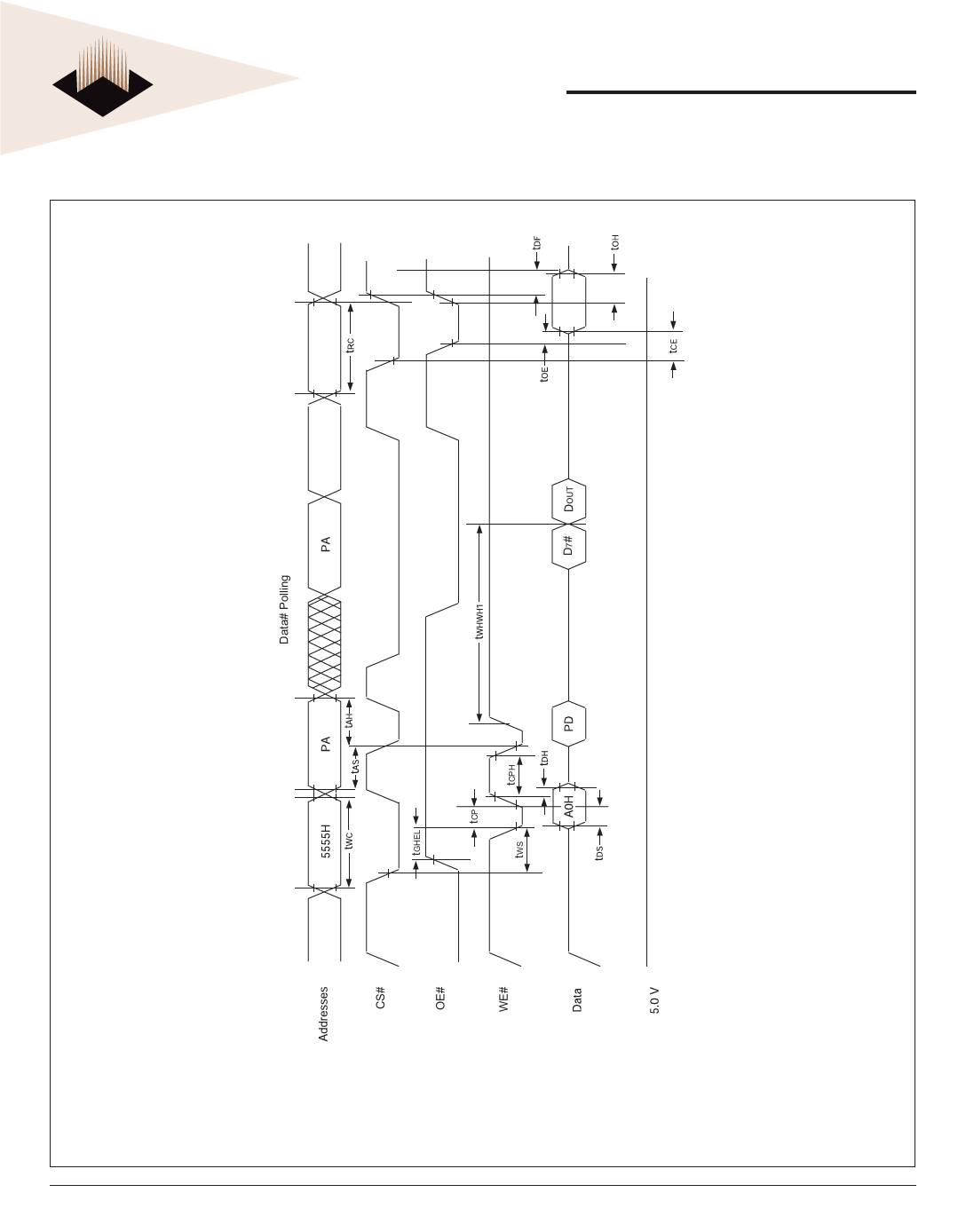
FIGURE 9 – ALTERNATE CS# CONTROLLED PROGRAMMING OPERATION TIMINGS
Notes:
1. PA represents the address of the memory location to be programmed.
2. PD represents the data to be programmed at byte address.
3. D7# is the output of the complement of the data written to each chip.
4. DOUT is the output of the data written to the device.
5. Figure indicates the last two bus cycles of a four bus cycle sequence.
October 2004
10
Rev. 5
White Electronic Designs Corporation • (602) 437-1520 • www.wedc.com
Share Link: 