SI-3000KM データシートの表示(PDF) - Sanken Electric co.,ltd.
部品番号
コンポーネント説明
メーカー
SI-3000KM
Sanken Electric co.,ltd.
SI-3000KM Datasheet PDF : 3 Pages
| |||
SI-3000KM Series
■Electrical Characteristics 2 (High Input Voltage type)
Parameter
Input Voltage
Output Voltage
(Reference voltage VADJ for SI-3010KM)
Line Regulation
Load Regulation
Dropout Voltage
Quiescent Circuit Current
Circuit Current at Output OFF
Temperature Coefficient of
Output Voltage
Ripple Rejection
Overcurrent Protection
Starting Current*2
Control Voltage (Output ON)*3
Control Voltage (Output OFF)*3
VC
Control Current
Terminal (Output ON)
Control Current
(Output OFF)
Input Overvoltage Shutdown Voltage
Symbol
VIN
VO (VADJ)
Conditions
∆VOLINE
Conditions
∆VOLOAD
Conditions
VDIF
Conditions
Conditions
Iq
Conditions
Iq (OFF)
Conditions
∆VO/∆Ta
Conditions
RREJ
Conditions
IS1
Conditions
VC, IH
VC, IL
IC, IH
Conditions
IC, IL
Conditions
VOVP
Conditions
SI-3010KM (Variable type)
min. typ.
2.4*1
max.
0.98 1.00
1.02
VIN=7V, IO=10mA
30
VIN=6 to 11V,
IO=10mA (VO=5V)
75
VIN=7V,
IO=0 to 1A (VO=5V)
0.3
IO=0.5A (VO=5V)
0.6
IO=1A (VO=5V)
600
VIN=7V, IO=0A, VC=2V
R2=10kΩ
1
VIN=7V, VC=0V
±0.5
Tj =0 to 100°C (VO=5V)
75
VIN=7V,
f=100 to 120Hz (VO=5V)
1.1
VIN=7V
2.0
0.8
40
VC=2V
–5
0
VC=0V
33
IO=10mA
SI-3050KM
min.
typ.
*1
Ratings
max.
min.
*1
SI-3090KM
typ.
max.
4.90
5.00
5.10
VIN=7V, IO=10mA
30
8.82
9.00
9.18
VIN=11V, IO=10mA
54
VIN=6 to 11V, IO=10mA
75
VIN=10 to 15V, IO=10mA
135
VIN=7V, IO=0 to 1A
0.3
IO=0.5A
0.6
IO=1A
600
VIN=7V, IO=0A,
VC=2V
1
VIN=7V, VC=0V
±0.5
Tj=0 to 100°C
75
VIN=7V,
f=100 to 120Hz
1.1
VIN=7V
2.0
0.8
40
VC=2V
–5
0
VC=0V
26
IO=10mA
VIN=11V, IO=0 to 1A
0.3
IO=0.5A
0.6
IO=1A
600
VIN=11V, IO=0A,
VC=2V
1
VIN=11V, VC=0V
±1.0
Tj=0 to 100°C
68
VIN=11V,
f=100 to 120Hz
1.1
VIN=11V
2.0
0.8
40
VC=2V
–5
0
VC=0V
30
IO=10mA
SI-3120KM
min.
typ.
*1
max.
11.76 12.00 12.24
VIN=14V, IO=10mA
72
VIN=13 to 18V, IO=10mA
180
VIN=14V, IO=0 to 1A
0.3
IO=0.5A
0.6
IO=1A
600
VIN=14V, IO=0A,
VC=2V
1
VIN=14V, VC=0V
±1.5
Tj=0 to 100°C
66
VIN=14V,
f=100 to 120Hz
1.1
VIN=14V
2.0
0.8
40
VC=2V
–5
0
VC=0V
33
IO=10mA
Unit
V
V
mV
mV
V
µA
µA
mV/ °C
dB
A
V
µA
µA
V
*1: Refer to the Dropout Voltage parameter.
*2: IS1 is specified at the 5% drop point of output voltage VO on the condition that VIN=overcurrent protection starting current, IO = 10 mA).
*3: Output is OFF when output control terminal (VC terminal) is open. Each input level is equivalent to LS-TTL level. Therefore, the device can be driven directly by LS-TTLs.
*4: SI-3010KM, SI-3050KM and SI-3090KM, SI-3120KM cannot be used in the following applications because the built-in foldback-type overcurrent protection may cause errors during
start-up stage.
(1) Constant current load (2) Positive and negative power supply (3) Series-connected power supply (4) VO adjustment by raising ground voltage
*5: VIN (max) and IO (max) are restricted by the relation PD = (VIN - VO) × IO. Please calculate these values referring to the Copper Laminate Area vs. Power Dissipation data as shown
hereinafter.
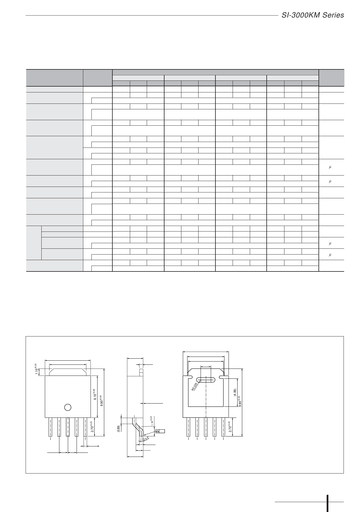
■External Dimensions (TO252-5)
(Unit : mm)
6.60±0.20
5.34±0.20
2.30±0.20
0.50±0.10
6.60±0.20
5.34±0.20
(5.04)
(1.50)
1.27 TYP
0.50±0.10
1.27 TYP
12345
SEATING PLANE
0.00 to 0.127
0.1
0 to 8°
0.50±0.10
(1.00)
2.30±0.20
Pin Assignment
q VC
w VIN
e GND
r VO
t Sense
(ADJ for SI-3010KM/SI-3120KM)
Plastic Mold Package Type
Flammability: UL94V-0
Product Mass: Approx. 0.33g
ICs 17
Share Link: 